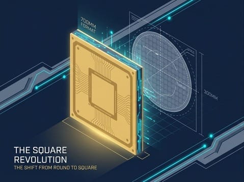
⭕ The Physical Chasm of Circles vs. Squares: Why Are Foreign Giants Collectively "Stymied"?
To understand the current boom among equipment manufacturers in Taiwan, we must first return to the fundamental physics of geometry.

For the past fifty years, the global semiconductor industry has operated on rules based on "circles." Whether it's Applied Materials and Lam Research in the United States or ASML in Europe, their robotic arms, vacuum chucks, and tracks—developed with billions of dollars in R&D—were all custom-built for "300mm diameter circular silicon wafers."
Now, Innolux and PTI have suddenly introduced an enormous 700mm \times 700mm "square glass" substrate.
For foreign giants, this isn't just a change in size; it means the "entire production line's physical logic must be re-engineered from scratch."
- Circular spin coater machines must be changed to square slot coaters.
- Mechanical arms designed to grip circular edges must be replaced with vacuum chucks that adhere to large square panels.
- What's more awkward is that FOPLP panel sizes are not yet standardized (some use 510mm \times 515mm, others use 700mm \times 700mm).
For foreign giants, redesigning and developing an entirely new set of "square equipment" for a new track where standards are not yet unified and the current market size is not substantial enough simply does not make financial sense in terms of Return on Investment (ROI).
Consequently, foreign giants have collectively adopted a wait-and-see approach, leading to stagnation.
⬛ The Absolute Home-Field Advantage of Dimensional Reduction: The Counterattack of Taiwan's "Square Table Players"
What foreign companies are unwilling or unable to do has become the "absolute home-field" for another group of hidden champions in Taiwan.
In Taiwan, there is a group of people who, for the past two or three decades, have never dealt with circular wafers but have consistently processed enormous "square PCB circuit boards" and "square LCD screens."
While semiconductor manufacturers pondered over the 700mm square table, these PCB/panel equipment manufacturers in Taiwan smiled:
"The PCB boards and TV panels we usually work with start at 1500mm \times 1500mm. You only need to work with $700mm$? That's a piece of cake for us!"
Leveraging their extensive experience in handling "large-area square substrates," these Taiwanese manufacturers, with a slight upgrade in cleanroom standards and micron-level precision, have directly entered the highest echelons of advanced packaging.
This is an epic "corner overtaking" maneuver.
🚀 Synonyms for Transformative Profits: Qunyi (6664) and Dongjie (8064)
In this wave of square-format arsenal, two key players are experiencing the most astonishing transformative profits.
Qunyi (6664) was originally a leading manufacturer of coating and baking equipment in Taiwan's PCB sector.
In FOPLP processes, large square panels require:
- Extremely uniform polymer material coating
- Long-duration precision baking (to control stress and warpage)
Leveraging its extensive experience with square-format equipment, Qunyi secured crucial orders from major OSAT (Outsourced Semiconductor Assembly and Test) manufacturers like ASE and PTI.
In the past, when manufacturing traditional PCB equipment, gross margins typically hovered around 30%.
However, since entering the high-end FOPLP and semiconductor advanced packaging markets, Qunyi's gross margin has surged past 45%, even nearing 50%.
This represents the ultimate transformative profit from transitioning from a "traditional industry" to a "semiconductor arms dealer."
As an equipment manufacturer within the same group as Innolux (part of the Foxconn/TECO system), Dongjie (8064) is the player with the most significant group synergy advantage in this battle.
Dongjie, originating from the panel industry, excels at:
- Handling large glass substrates
- Laser repair
In FOPLP production lines, Dongjie is not only responsible for factory-wide Automated Material Handling Systems (AMHS) and square cassettes, but has also proactively positioned itself in the future glass core substrate market with core TGV (Through-Glass Via) laser equipment.
They are leveraging the formidable transformative power of their group's panel factories, becoming a crucial external aid in this wave of square-format factory construction.
🚪 A Perfect Transition: Can Taiwanese Manufacturers Only Do "Handling" and "Baking"?
Having understood this physical shift between "circles" and "squares," we've witnessed how Qunyi and Dongjie have leveraged their home-field advantage to capture the construction dividends that foreign companies cannot access.
However, there has always been a dismissive sentiment towards Taiwanese manufacturers in the market:
"These equipment manufacturers in Taiwan are, frankly, just making 'peripheral equipment' like ovens and glass handlers. The core process tools that truly determine the life or death of a chip and involve the highest technical difficulty, such as 'vacuum thin-film deposition (PVD/ALD),' still depend on the whims of foreign companies, don't they?"
This was certainly true in the past.
But this time, the FOPLP revolution has given rise to a group of true dark-horse technology beasts in Taiwan: they have not only broken the absolute blockade of foreign companies in "vacuum equipment" but have also independently developed the world's first "panel-level Physical Vapor Deposition (PVD)" machine.
🌌 The Toughest Hurdle: Vacuum Thin-Film Deposition (PVD) and the Physical Nightmare of Square Plasma
To understand the greatness of Tianhong, we must first comprehend the most challenging physical hurdle in semiconductor manufacturing processes: Film Deposition.

In advanced packaging, we need to lay layer upon layer of extremely thin, extremely uniform metal conductive layers between the chip and the substrate.
This cannot be achieved by traditional coating methods; it must be done in a "high-vacuum environment," where special gases are introduced and excited to produce high-energy plasma, causing metal atoms to precisely bombard and deposit onto the substrate like falling snow.
This is PVD (Physical Vapor Deposition).
For the past thirty years, this black magic of plasma control has been tightly monopolized by giants like Applied Materials from the US and ULVAC from Japan.
However, when FOPLP (Panel-Level Packaging) emerged, these foreign giants collectively shook their heads.
The reasons are:
- Controlling plasma uniformity in a "circular" chamber is already extremely difficult.
- Now, the requirement is to perform vacuum PVD in a giant square chamber.
In the four corners of a square chamber, airflow and electromagnetic fields create extremely complex edge effects, leading to uneven film thickness.
For foreign giants, who do not lack orders, redeveloping fluid dynamics and electromagnetic field models for a square market with unstandardized dimensions simply does not yield sufficient R&D benefits.
⚡ The Wall-Breaker Arrives: Tianhong (6937)'s World's First Panel-Level PVD
Just as FOPLP production lines in Taiwan faced bottlenecks due to the lack of "square vacuum equipment," Tianhong Technology (6937), founded by a group of top engineers from former US-based equipment manufacturers, broke through with its indigenous black technology.
They chose not to compromise but to directly challenge the most difficult physics.
Tianhong successfully overcame the challenges of airflow and plasma distribution in square chambers, independently developing:
The world's first 310mm \times 310mm panel-level PVD equipment
(and is already capable of tackling larger sizes)
The strategic significance of this machine is that:
- It proves that equipment manufacturers in Taiwan have moved beyond the low-end comfort zone of "peripheral handling."
- Taiwanese companies have officially entered the "core vacuum process" field, which boasts the purest gold content.
As Innolux and PTI prepare to build extremely fine, high-density Redistribution Layers (RDL) on square glass, they finally possess a fundamental arsenal that is fully controlled by local expertise, capable of "deeply customized fine-tuning" parameters at any time to address production line issues.
⚛️ The Ultimate Weapon for the Future: ALD Atomic Layer Deposition and the Foreshadowing of Silicon Photonics (CPO)
If Tianhong were to stop at PVD, it would, at best, only be an excellent alternative supplier.
However, based on our think tank's in-depth analysis of its technology roadmap, Tianhong's ambition is already set on the ultimate battlefield of the next decade: ALD (Atomic Layer Deposition).
- From "Snowfall" to "Tile Laying":
If PVD is like covering metal with snow, then ALD is precisely "laying tiles" layer by layer at the atomic level.
Even in vertical deep holes with extremely exaggerated aspect ratios (such as future TGV (Through-Glass Via) holes in glass substrates), ALD can still ensure that every wall is uniformly coated with a film of absolutely equal thickness.
- The Hegemony of Next-Generation Applications:
According to the latest industry intelligence, Tianhong's ALD equipment has begun to be fully introduced into Micro LED display technology for the passivation protection layers of extremely tiny chips.
Even more impressively, Tianhong's reach has extended to EUV inspection and coating equipment, as well as CPO (Co-Packaged Optics) silicon photonics, which will address the transmission limits of AI chips in the future.
Tianhong's strategic value is no longer merely the localization of equipment in the traditional sense.
It is building a completely independent and self-reliant "high-vacuum microscopic arsenal" for Taiwan's advanced packaging, next-generation display technology, and future silicon photonics revolution, free from the control of European, American, and Japanese giants.
🧪 The Collapse of Thirty Years of Material Hegemony: The "Circular Failure" of Japan's Patent Wall
If you recall the "chemical chokehold warfare" we mentioned in 5-2-6, you'll know that in the world of advanced packaging for traditional 12-inch silicon wafers, Japanese material giants (such as Ajinomoto ABF, Sumitomo Chemical, and Shin-Etsu Chemical) held absolute dominance.
They spent thirty years weaving a dense web of patent protection specifically for "silicon wafers" and "circular processes."
In the past, whenever material manufacturers in Taiwan ventured into advanced packaging, they often immediately ran into Japan's patent wall, rendering them immobile.
But when FOPLP shifted the battlefield to enormous 700mm square glass, a miracle occurred:
Many material patents and physical formulations originally applied to 12-inch circular silicon wafers instantly became ineffective on large square glass.
The thermal expansion coefficient of glass is different from silicon, and the fluid dynamics of large-area coating also differ from small circular disks.
Foreign giants suddenly discovered that their proudly developed old formulations would severely warp or even crack when applied to large square panels.
The rules of the game were reset, forcing everyone back to the same starting line.
🔄 The Golden Age of Dimensional Shift: The Historic Counterattack of Taiwan's PCB Material Manufacturers
While Japanese giants were frantically revising their formulations in the laboratory, a group of people in Taiwan smiled knowingly.
This group comprises Taiwan's traditional PCB (Printed Circuit Board) material manufacturers.
For decades, they have been researching:
- How to precisely lay copper foil on a large square board
- How to inject plating solutions
- How to apply insulating materials
When it comes to controlling chemical stress over large, square areas, chemical manufacturers in Taiwan possess even richer experience than those lofty Japanese semiconductor material companies.
This is a true "dimensional shift."
- Chang Chun Petrochemical: The hidden global leader in PCB copper foil and plating solutions, directly transferred its high-end plating solution technology to the micron-level copper wiring deposition for panel-level packaging.
- Nanya Plastics / TAIWAN UNION TECHNOLOGY CORPORATION (2383): Originally major manufacturers of CCL (Copper Clad Laminate) and dielectric materials, they are now leveraging their deep foundation in processing large square substrates to aggressively enter the material supply chain for FOPLP and future glass substrates.
Taiwanese material manufacturers have finally found a historic opportunity to bypass thirty years of Japanese patents and directly penetrate the core profit zone of semiconductor packaging.
💀 Alarm Bell: The "Death Valley" of Yield Rates
Analyzing up to this point, the prospects for FOPLP seem excellent. Equipment manufacturers are making a fortune, and material suppliers are also poised for a corner overtaking.
However, we absolutely do not advocate blind optimism.
At this moment, we must sound the most severe alarm bell for this idolization: Behind this FOPLP craze lies a "death valley" that could bankrupt countless panel manufacturers.
On paper, FOPLP's area is 7 times larger, and costs can be reduced by two-thirds (30% of original cost). However, in a real cleanroom:
- The Extreme Fragility of Glass:
A 700mm ultra-thin glass substrate can instantly shatter with even a slight collision or uneven heating.
If one piece of glass breaks, thousands of chips on it are destroyed with it, leading to devastating losses.
- Insoluble Giant Warpage:
The larger the panel, the more terrifying the accumulation of thermal stress.
After materials are coated and placed in the oven, the warpage deformation at the edges can be as high as several millimeters, making it impossible for subsequent micron-level lithography machines to align properly.
The biggest risk for FOPLP has never been the inability to procure equipment, but rather "yield ramp-up."
This is not a risk-free highway.
Within the next two to three years, there will undoubtedly be panel manufacturers or OSAT companies lacking sufficient capability that will be forced to withdraw in a bottomless money-burning quagmire, simply because they cannot raise their yield rates to an acceptable level.
This is a cruel survival battle where only the fittest survive: whoever can first cross the death valley of yield rates will exclusively enjoy the formidable pricing power and monopolistic profits of "one-third the cost."
In-depth Research · Quantitative Perspective
Want to gain more insights into semiconductor quantitative research?
【Insight Subscription Plan】Break Free from Retail Investor Mentality: Build Your Alpha Trading System with "Quantitative Fund Flow" and "Consensus Data"EDGE Semiconductor Research
📍 Series Map — Navigate the Complete EDGE Semiconductor Research →


