NVIDIA: ABF substrate pain point → CoWoP substrate-less (direct-to-PCB)
⛓️ The Giant's Circular Cage: CoWoS's Ultimate Physical Ceiling
To understand why TSMC must launch this ultimate "transforming circles into squares" mutation, we must first confront an imminent, unsolvable physical deadlock under the current surge in AI computing power: CoWoS's reticle limit and area curse.
TSMC's CoWoS (Chip-on-Wafer-on-Substrate) is currently the most powerful 2.5D packaging technology on Earth.
Its approach involves laying out GPU computing cores and HBM (High Bandwidth Memory) on a silicon interposer made from a "12-inch circular silicon wafer."
However, AI chips are becoming increasingly massive at an uncontrollable pace.
In pursuit of ultimate computing power, NVIDIA and AMD are aggressively cramming more transistors and more HBM into the same package.
Here is a specialized term in the semiconductor industry: Reticle Limit, which is approximately 858 mm^2.
A few years ago, AI chips had a package area of roughly 1–2 times the reticle limit.
Today's NVIDIA B200 has a package area approaching 3.3–4 times the reticle limit.
For the future Rubin generation and even the next generation of giants, the industry estimates that package area will break through 5.5 times, or even 8 times, the reticle limit.
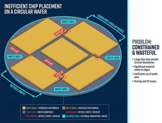
This presents a geometric disaster:
TSMC's base is a circular silicon wafer with a diameter of 300mm (12 inches).
When you need to cut a super interposer with an area as large as 5.5 times the reticle limit (equivalent to an extra-large rectangular lunchbox) from this circular wafer:
You will find that almost all of the irregular edge space becomes waste.
Calculating across an entire wafer, only a mere "single-digit number" of complete super interposers might be cut.
This is no longer a yield issue; it's a complete collapse of "physical area utilization rate."
Under such extreme waste, the packaging cost of future-generation super AI chips could skyrocket to levels even cloud giants (Microsoft, Google, Meta) find unbearable.
The development of AI computing power is on the verge of being firmly trapped by this "12-inch circular cage."
⬛ The Ultimate Beast Breaking Boundaries: CoPoS Arrives
Facing the impending physical deadlock, TSMC has presented an extremely aggressive and shocking ultimate solution:
"If a 12-inch circular wafer cannot accommodate future giants, then replace the base with an infinitely large square panel."
This is the ultimate mutation weapon hidden deep within the technology roadmap: CoPoS (Chip-on-Panel-on-Substrate).
It retains the Chip and Substrate components of CoWoS, but forcibly replaces the Wafer, which represents a 12-inch wafer, with the Panel, which represents a large square glass/panel.
TSMC will abandon traditional 12-inch circular silicon wafer equipment, introducing ultra-large square substrates, possibly high-end organic materials or the glass substrates mentioned in the previous chapter, with sizes up to 510mm \times 515mm, or even 700mm \times 700mm.
This will bring two fundamental changes:
Liberation of expansion space: The panel is virtually no longer restricted by circular edge waste, allowing for larger-area giants.
Crushing cost reduction through scale: Area utilization can be significantly increased, raising single-run output from "a few units" to "dozens of units," using economies of scale to suppress packaging costs.
Therefore, FOPLP is by no means exclusive to low-end automotive chips.
When TSMC "transfers" its decade of accumulated CoWoS nanometer-level precision routing technology (RDL) directly onto massive square panels, this is a "panel-level extravaganza" reserved exclusively for the AI giants at the very apex of the pyramid.
⏳ Strategic Timeline: VisEra's Experimentation Line and the Ambition of Chiayi AP7
This is not science fiction merely on paper.
This post is for subscribers only
Sign up now to read the post and get access to the full library of posts for subscribers only.