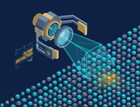
Welcome to the first trial gate in the "six realms of reincarnation" for AI chips. Before the chip is put through its paces with hundreds of watts of current, pushed "to its limits," we must first use our "eyes" to confirm its physical structure is perfect.
This task is entrusted to AOI (Automated Optical Inspection).
In the era of traditional PCBs (Printed Circuit Boards), AOI was like a traffic cop catching violations on flat ground. But in the microscopic world of CoWoS advanced packaging, AOI faces a "nerve-wracking" 3D revolution.
🏙️ The 3D Revolution: A Needle in a Haystack, from 2D to 3D
Imagine this scenario: we place ten "Taipei 101" skyscrapers side-by-side, and then ask you to find, within 3 seconds, which one of the screws on the exterior wall of these ten buildings is loose by half a millimeter.
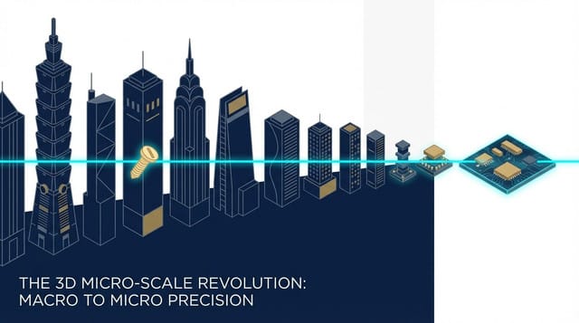
This is what AOI equipment does every day in advanced packaging.
In CoWoS or FOPLP (Fan-Out Panel Level Packaging) processes, the spaces between chips, and between chips and substrates, are filled with hundreds of thousands, or even millions, of "Micro Bumps." These bumps are only one-tenth the diameter of a human hair. If just one of these bumps has a tiny crack or is slightly off by a few micrometers, the entire million-dollar AI chip will be directly scrapped in subsequent high-temperature tests.
Previously, AOI performed "2D inspection," which meant taking a flat photo from above to check if any bumps were missing.
But that's no longer sufficient. Micro bumps are too small and dense; engineers must know if the "height" of these hundreds of thousands of bumps is absolutely consistent (Coplanarity). If even one bump is 2 micrometers too short, the chip might not make proper contact, leading to an open circuit or short circuit.
Therefore, AOI equipment was forced to undergo an epic "3D revolution."
Today's high-end AOI not only takes photos but also projects extremely precise laser gratings, utilizing optical interference principles to instantly measure the 3D volume and height of millions of bumps. This places almost impossibly stringent demands on optical lens resolution and image processing power.
💸 Capital Sinkholes and the "Mathematics of Yield"
If you examine the capital expenditure (CapEx) reports of TSMC or ASE, you'll notice a startling phenomenon: in advanced packaging plants, the procurement amount for AOI-related equipment accounts for 15% to 20% of total CapEx, almost second only to the most expensive photolithography equipment.
Why does mere "inspection" cost so much? AOI is practically a "money shredder" in a packaging plant.
The answer lies in the brutal "mathematics of yield."
Suppose advanced packaging has three critical steps:
- Micro Bump formation
- Redistribution Layer (RDL) fabrication
- 3D Chip Stacking
If the yield for each step is a "seemingly good" 90%, then the final yield would be:
The final yield is only 72%! Nearly 30% of top-tier AI chips would be discarded, a loss in the tens of billions of New Taiwan Dollars.
How do packaging plants forcefully push that 72% back up to over 95%?
The only solution: "Inspect after every step."
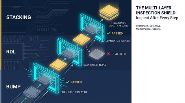
After Bump formation, one AOI inspection; after RDL fabrication, another AOI inspection; after chip attachment, yet another AOI inspection. As soon as a defect is found, it's immediately removed for scrap or rework, ensuring that defective semi-finished products never enter the next expensive process.
Because the number of "inspection points" has increased from 1 to 3, or even 5, the procurement quantity of AOI machines naturally multiplies. This is the ultimate source of exorbitant profits for AOI equipment manufacturers.
🧠 The Truth About Moats: The Severely Imbalanced "Data Flywheel"
Witnessing the explosion in AOI equipment demand, many companies traditionally focused on camera modules or general industrial inspection want a piece of the pie. They mistakenly believe: "If I just buy the best German lenses and run AI image recognition on the latest Nvidia GPUs, I can do semiconductor AOI."
This is a fatal misjudgment.
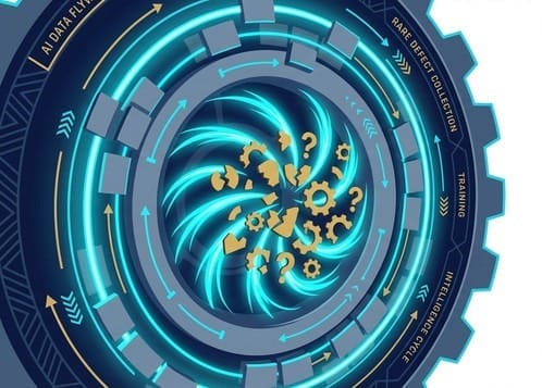
In the AOI battlefield for high-end packaging, the most challenging aspect has never been "clear imaging," but rather the "AI algorithm's data flywheel."
It's important to understand that TSMC and ASE already achieve very high yields. On a production line, out of a million micro-bump images captured, perhaps only "3" actually show defects.
In machine learning, this is referred to as "Extreme Class Imbalance."
- If the model hasn't seen enough "images of genuinely defective chips," it won't learn how to identify flaws.
- It will either fail to detect defects (missed detection, leading to customer losses).
- Or it will constantly raise false alarms (false positives, identifying good chips as bad, causing yield figures to plummet).
Therefore, AOI's most impenetrable moat is "time and trust."
This AI image model is "not for sale." It must be moved into the cleanroom of a top-tier packaging plant, run day and night alongside the production line, absorbing countless real defect data points, and only after two to three years of continuous "feeding" and "fine-tuning" will the data flywheel begin to spin.
Whoever can first get major clients to approve and move their equipment into the factory to begin collecting these "highly confidential defect images" will be able to train the smartest AI models, effectively sidelining latecomers.
⚔️ Breakthrough Paths of the Four Detection Giants: Who Holds the Key?
In this battle, transitioning from PCB into semiconductor advanced packaging, the following four hidden champions each hold different trump cards and face distinct risks.
1) UTECHZONE (3563): The Privileged Player Leveraging Key Alliances
- Strategic Positioning: Absolute leader in PCB AOI, made an extremely astute and market-shaking decision: introducing global OSAT leader "ASE Technology Holding (3711)" as its largest private equity shareholder.
- Insight (Moat and Flywheel): This is equivalent to receiving a "golden ticket." While other equipment providers are still vying for data outside, UTECHZONE's machines have already entered ASE's cleanrooms, commencing the absorption of the most authentic 3D packaging defect data.
- Risk Factor: Extreme customer concentration. The success or failure of its semiconductor transition is almost entirely tied to ASE's orders and expansion pace.
2) TRI (3030): The Heavy Infantry Leveraging Channels to Attack Upstream
- Strategic Positioning: A veteran in global PCBA (Printed Circuit Board Assembly) inspection, possessing strong sales channels and cash flow, now directly targeting packaging with 3D optical inspection technology accumulated from SMT production lines.
- Insight: Its advantage lies in its "ability to offer integrated solutions," providing comprehensive offerings from 3D SPI (Solder Paste Inspection) to 3D AOI, and even X-Ray. This is attractive to OSATs that prefer not to be locked into a single vendor.
- Risk Factor: Semiconductor microphysics (nano/micrometer scale) and PCBA (millimeter scale) are two different worlds, requiring overcoming a steep learning curve.
3) TOPCO (3167): The Cross-Industry Dark Horse with a Square-Panel Home-Field Advantage
- Strategic Positioning: Originally deeply rooted in PCB equipment and inspection, its home-field advantage has actually amplified under the FOPLP (Fan-Out Panel Level Packaging) trend.
- Insight: When packaging substrates transition from "round" to "extra-large square panels" of approximately 700mm, traditional semiconductor AOI manufacturers face challenges. Leveraging its extensive experience in large-format square PCB and panel AOI, TOPCO has rapidly penetrated the FOPLP inspection supply chain, forming a "three-way rivalry" with UTECHZONE and TRI.
4) Promate Solutions Inc. (6816): The Software Specialist with a Pure-Play AI Brain
- Strategic Positioning: A pure-play AI image software and algorithm company, asserting "We don't make machines; we only provide the intelligence."
- Insight: Specializes in solving the problem of "extremely imbalanced defect samples," and through alliances with major equipment manufacturers, implants defect detection models directly into production lines.
- Risk Factor: Friction in software-hardware integration. If image quality is unstable, clients often attribute the responsibility to the software, requiring proof that the algorithms are compatible with various hardware environments.
🗺️ Strategic Conclusion: AOI is the First Filter in Advanced Packaging
In summary, these four companies are capturing the massive capital expenditure (CapEx) released by TSMC and ASE as they strive to improve yield rates.
The logic behind investing in these AOI equipment stocks is also clear: as the number of layers in advanced packaging (CoWoS, FOPLP, SoIC) continues to increase, the number of required "photographic inspections" in between will multiply exponentially, leading to an virtually limitless revenue ceiling.
In-depth Research · Quantitative Perspective
Want more quantitative research insights on semiconductors?
[Insight Subscription Plan] Bid Farewell to Retail Investor Mindset: Build Your Alpha Trading System with 'Quantitative Flows' and 'Consensus Data'EDGE Semiconductor Research
📍 Series Map — Navigate the Complete EDGE Semiconductor Research →


