Topic: The Ultimate Forensic Examiner – Microscopic Dissection Platforms and the "Big Three" in Material Analysis and Testing
Keywords: AOI Blind Spots, FA/MA, FIB, TEM, Sample Preparation, Localization (JASM/Rapidus), RA (Reliability Analysis), AI Server System-Level Verification
In 5-4-1, we stated that AOI (Automated Optical Inspection) is the first filter in advanced packaging. However, AOI has a fatal physical blind spot: it can only see the "surface"!
AOI is like a drone flying outside a newly constructed building, checking for cracks on the exterior walls or crooked windows. But what if the "rebar" inside the building is rusted? What if the "sand-to-cement ratio" in the concrete is incorrect? A drone would absolutely not be able to tell.
As TSMC enters the era of 2nm GAA (Gate-All-Around) transistors and 3D CoWoS advanced packaging, the internal three-dimensional structure of chips has become complex to an "atomic level." When a chip fails during earlier FT (Final Test), SLT (System-Level Test), or Burn-in, or when TSMC's new process yield suddenly drops from 80% to 50%, the entire supply chain falls into extreme panic.
At this point, merely relying on AOI images or machine test data can no longer identify the cause of death. We must call upon the semiconductor industry's coldest "ultimate forensic examiner" – Independent Testing Labs.
🔪 Microscopic Dissection Platform: "Cutting Open" Chips Worth Tens of Thousands of US Dollars
When failed chips are sent to these laboratories, they are not met with electrical tests, but with a horrifying "microscopic autopsy."
This is the battlefield of FA (Failure Analysis) and MA (Material Analysis):
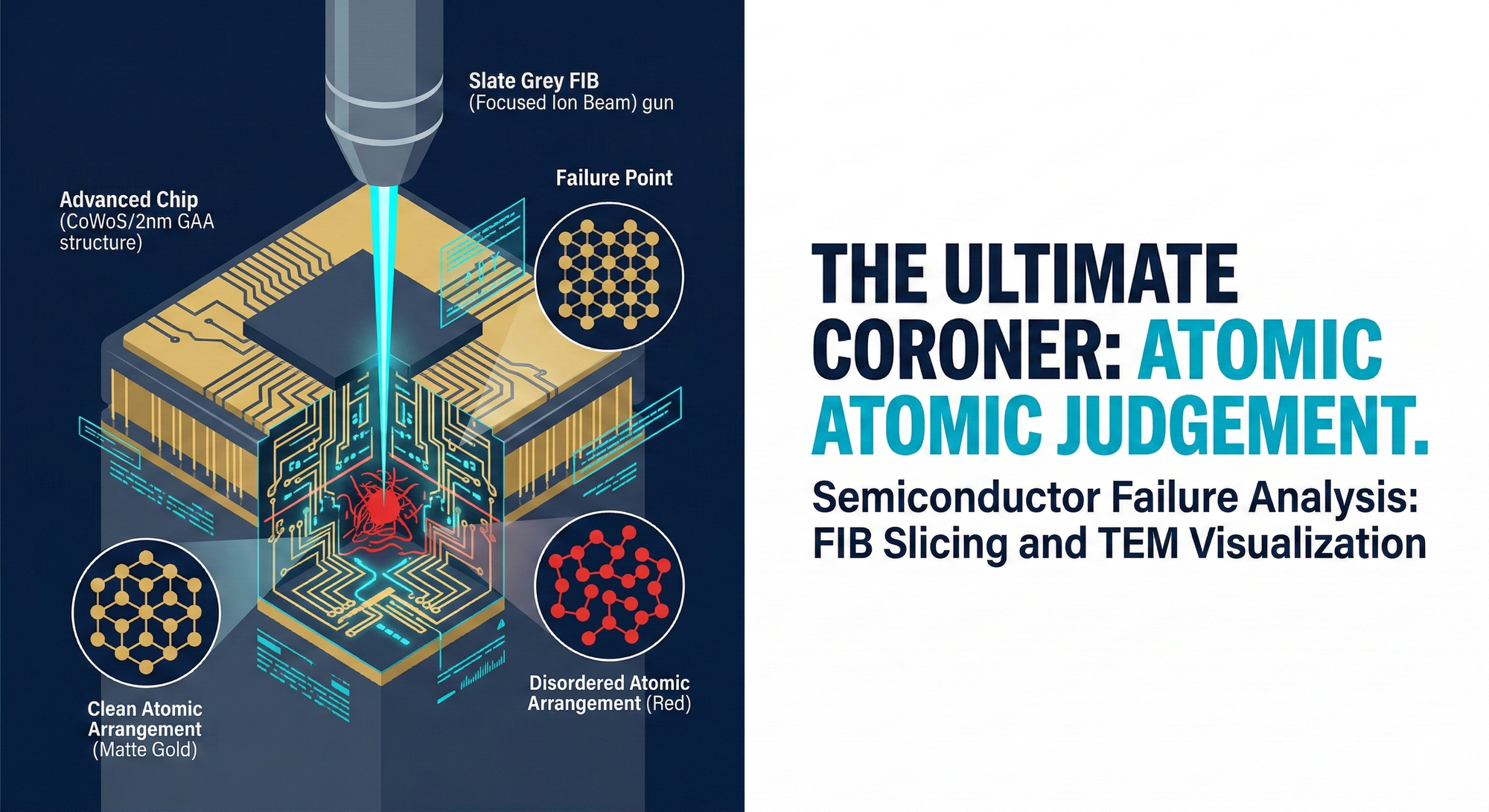
- FIB (Focused Ion Beam) Precision Cutting: Engineers use FIB machines costing hundreds of millions of New Taiwan Dollars, emitting high-energy gallium ion beams like extremely sharp nanoscale scalpels, precisely "vertically cutting open" the location on the chip where a short circuit occurred.
- TEM (Transmission Electron Microscope) Atomic-Level Perspective: After cutting, engineers place the slice, which is only a few atoms thick, under an electron microscope. At this point, the chip's internal 3D structures, the "cross-sections" between different metal layers, and even the arrangement of atoms are all revealed clearly on the screen.
This is the ultimate method for "finding the cause of death."
Engineers might discover under the microscope that the gate oxide layer of a 2nm transistor has a non-uniform thickness of 1nm; or that microbumps in a CoWoS package developed abnormal intermetallic compounds (IMCs) between two metals after high-temperature baking at 125°C, leading to microscopic fractures.
💰 The Profitable Business of Selling "Answers": The Shovel Sellers in the R&D Arms Race
This is an extremely expensive business. These testing laboratories must invest billions of New Taiwan Dollars to acquire the world's most advanced electron microscopes and analytical equipment; concurrently, they must hire "forensic examiners (analysis engineers)" with master's or doctoral degrees and top-tier material physics backgrounds.
However, their business model is incredibly appealing. They don't sell machines, they don't sell consumables; they sell "answers"!
TSMC, MediaTek, and NVIDIA are willing to pay extremely high fees for an analysis report that precisely identifies the cause of death and includes high-resolution electron microscope images. Because as long as the cause of death can be found, and process parameters can be modified to increase yield by 1%, the money saved for clients is measured in "billions of New Taiwan Dollars"!
This also means: the performance of testing laboratories does not depend on the economic climate of end-products, but solely on "R&D complexity."
As long as TSMC is pushing hard to develop A16 and A14 processes; as long as NVIDIA is frantically experimenting with new 3D packaging materials and silicon photonics (CPO) technology, engineers will continue to make mistakes, chips will continue to fail, and these laboratories will have an endless stream of cases.
🗡️ PSMC (6830): The "Imperial Blade Master" Guarding the Nanometer Frontier
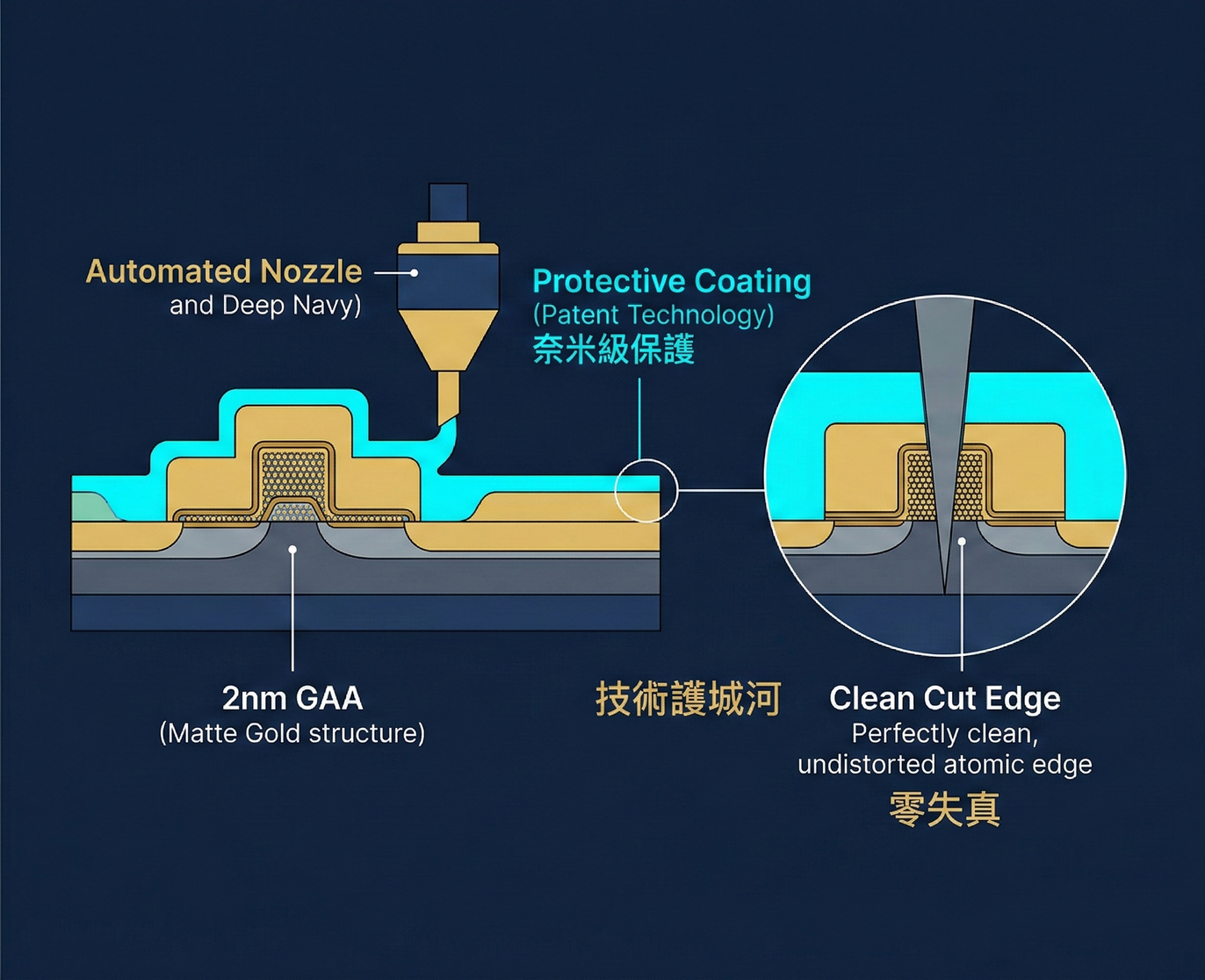
To find the cause of death in 2nm or even A16 processes, the first step is to "cut open" the chip. This sounds simple, but in the atomic-level world, it is an extremely difficult physical challenge.
When you use a high-energy Focused Ion Beam (FIB) to cut transistors that are only a few nanometers wide, the high temperature and impact force of the ion beam can easily "melt" or "distort" the inherently fragile structure. If you damage the sample itself, what you see under the electron microscope will only be a distorted piece of scrap metal, making it impossible to find the true cause of death.
PSMC (6830)'s absolute moat is its "god-tier" sample preparation technique.
They possess exclusive patented technologies for "low-temperature atomic layer deposition" and "conductive adhesive." Before cutting the chip, they apply an ultimate protective layer to ensure that the atomic structure does not deform during ion beam cutting.
Think Tank Strategic Positioning: [MA (Material Analysis) Overlord in Advanced Processes] PSMC has chosen the "most hardcore" path. It has concentrated the vast majority of its resources on the most challenging and most expensive MA (Material Analysis) domain. Due to its precise "blade work," PSMC has become the indispensable "imperial anatomist" for TSMC, the "sacred mountain" of the industry, as it advances 3nm, 2nm, and silicon photonics R&D. As long as TSMC's Moore's Law continues to progress, PSMC's MA orders will be endless.
🌍 MA-Tek (3587): The "Global Pioneer" Benefiting from Japan's Resurgence
If PSMC is the blade master guarding the advanced process frontier in Hsinchu and Tainan, then MA-Tek (3587) is the "global pioneer" planting flags everywhere in the Age of Discovery.
MA-Tek has the most balanced presence across MA (Material Analysis), FA (Failure Analysis), and RA (Reliability Analysis). However, its true strength, which earns it high valuations from the capital market, lies in its extremely keen "geopolitical intuition."
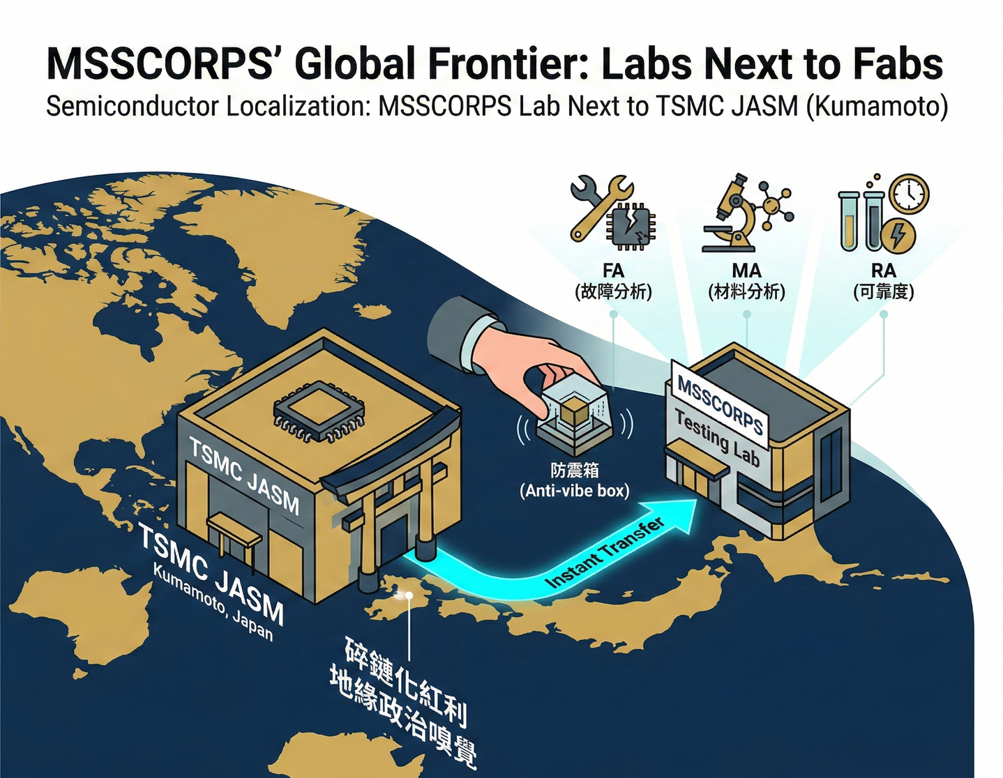
There is an iron rule in semiconductor testing and analysis: "Samples cannot stay overnight, analysis cannot wait." When a wafer fab production line encounters issues, clients expect engineers to deliver chips to the lab in anti-vibration boxes within half an hour and receive an autopsy report on the same day. Therefore, laboratories must be built alongside wafer fabs.
Think Tank Strategic Positioning: [The Biggest Winner of Semiconductor Localization]
When TSMC decided to build a plant in Kumamoto, Japan (JASM), MA-Tek was the first Taiwanese company to unhesitatingly follow suit and establish a top-tier laboratory in Japan.
As the Japanese government is dedicating national efforts to revive its semiconductor industry (including Rapidus' 2nm plan), Japan's domestic market severely lacks modern third-party testing laboratories. As soon as MA-Tek's Kumamoto lab opened, it was almost instantly overwhelmed with orders from Japanese automakers and chip manufacturers.
Beyond Japan, MA-Tek's laboratories in mainland China have also fully capitalized on the massive dividends from China's semiconductor "de-Americanization and indigenous R&D" efforts. Investing in MA-Tek means investing in the major global trend of semiconductor supply chain "fragmentation and localization."
🚗 iST (3289): The Master of Extreme Environment Stress and "System-Level Bodyguard"
Finally, let's look at iST (3289). This company's strategic blueprint fundamentally differs from the previous two.
While PSMC and MA-Tek expend significant effort on "observing" atomic arrangements, iST places its heaviest emphasis on RA (Reliability Analysis) and signal testing.
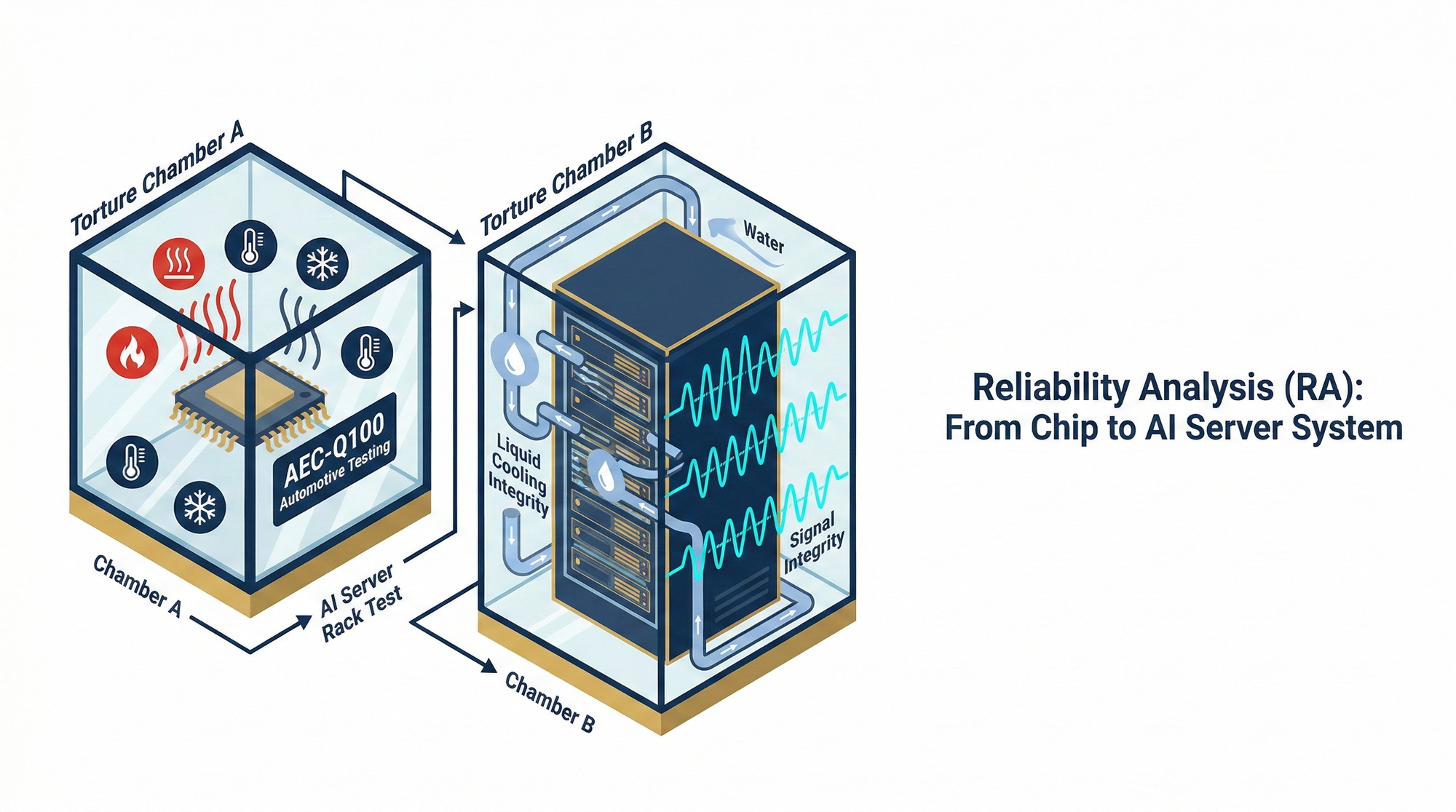
What is reliability analysis? It's about subjecting chips or entire devices to brutal treatment in extremely harsh environments!
For example, automotive chips must pass the extremely stringent AEC-Q100 certification. iST's laboratories are filled with high and low-temperature shock testers, vibration test stands, and even highly humid and high-pressure chambers. Automotive chips must endure thousands of hours of torment in these "torture devices" to prove they won't fail in deserts or snowy conditions ranging from -40°C to 150°C, thus earning the right to be adopted by car manufacturers.
Think Tank Strategic Positioning: [The King of AI Server and Automotive Electronics System-Level Verification]
In the AI era, iST's battlefield has expanded from "individual chips" to "entire AI servers."
When all components of an AI server, such as PCIe Gen6 transmission cables, high-speed switches, and liquid cooling modules, are assembled, will this monster, costing tens of millions, leak? Will high-frequency signals attenuate?
iST not only cuts chips but also assists contract manufacturers like Quanta and Wistron in performing "Signal Integrity" and "Thermal Reliability" verification for entire systems. iST acts as the strongest bodyguard, the final gatekeeper before AI system manufacturers ship their products.
🗺️ Think Tank's Ultimate Conclusion: Chapter 5-4 Ends, Prepare to Enter the "Sixth Battle Zone"!
With the strategic landscapes of the "Big Three" in testing completed, we finally draw a perfect close to this vast [5-4 The Violent Aesthetics of Testing and the Consumables Holy War]!
Let us take a bird's-eye view and review this thrilling journey:
- King Yuan Electronics (2449) showed us the money-printing machine effect of exponentially increasing "test time" for AI chips.
- MPI (3563) and other AOI leaders used 3D stereo lasers to detect microscopic cracks on the surface of advanced packages.
- MPI Corp. (6223) and CHPT (6510) launched microscopic assassinations with 112G high-frequency MEMS probe cards on wafers; while UNIMOS (6683) provided robust steel rings, and Santec (3595) was responsible for cleaning up battlefield debris.
- InGrasys (6515) created a "coaxial throne" capable of withstanding 1000W power consumption and 150°C high temperatures, and ventured into the SLT blue ocean with HyperSocket.
- Chroma (2360) demonstrated the ATC magic of locking temperature within 50 milliseconds during SLT combat drills.
- Hong Jing (7769) challenged the limits of thermal expansion in mechanical handling within 125°C Burn-in ovens.
- Finally, PSMC, MA-Tek, and iST cut open chips, using electron microscopes to peer into the ultimate mysteries of semiconductor life and death.
This testing supply chain is the "absolute high-profit zone" within the entire AI semiconductor industry, characterized by the highest gross margins, clients least likely to demand price cuts, and the most frequent replacement of consumables.
In-depth Research · Quantitative Perspective
Want more insights from semiconductor quantitative research?
[Insight Subscription Plan] Bid Farewell to Retail Investor Mindset: Build Your Alpha Trading System with "Quantitative Capital Flows" and "Consensus Data"EDGE Semiconductor Research
📍 Series Map — Navigate the Complete EDGE Semiconductor Research →


