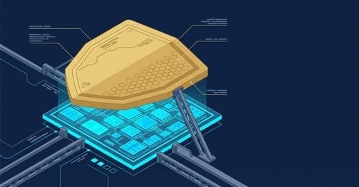
6-3-1 Metal Bodyguards for Chips: Kenmec (3653) and Flatness Anxiety in the CoWoS Era
In the CoWoS era, heat spreaders are critical for AI chip protection. Kenmec (3653) uses 'precision cold forging' to overcome warpage, achieving micron-level flatness for optimal heat dissipation and yield. Its one-stop plating/stiffener frame service grants strong pricing power, a semiconductor ...
🏗️ More Than Just a Lid: The "Heavy Armor" for CoWoS's Delicate Princess
Why do we need an IHS? If it's just for heat dissipation, why not let the water block press directly onto the chip (Direct Die Cooling)? Wouldn't that result in lower thermal resistance?
In the era of traditional small chiplets, this might work. But in NVIDIA's CoWoS advanced packaging era, this would absolutely be a suicidal act. Recall the Blackwell architecture we saw in Chapter 5: two massive GPU dies in the center, surrounded by eight extremely fragile HBM (High Bandwidth Memory) modules, all resting on a silicon interposer that is more brittle than an eggshell.
This is an extremely delicate combination. There is often a micron-level height difference between the HBM and the GPU. If you press a water block weighing several kilograms directly onto it, even slight unevenness in pressure can cause an HBM module to directly "chip" or "crack." If one HBM module breaks, the entire B200, valued at forty thousand US dollars, becomes scrap.
Therefore, we need an "intermediary." This intermediary must be able to withstand the immense clamping force of the heatsink while protecting the fragile wafer structure below. This is the strategic role of the IHS (Integrated Heat Spreader). It is not just a thermal conduction bridge; it is the "heavy armor" for CoWoS chips. In the industry's definition, it has evolved from a simple "thermal component" to a "critical packaging material" that safeguards chip yield.
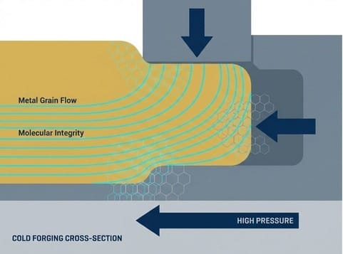
🔨 The Art of Forging: Why Stamping Has Been Eliminated
Since an IHS is a copper lid, why not just find any stamping factory that makes pots and pans to produce it? Wrong. This is precisely why only Kenmec (3653) in Taiwan can manufacture it, while other metal processing factories can only look on from the sidelines.
Based on our in-depth analysis of the metal processing industry chain, traditional stamping processes face two critical physical limitations in the AI era:
Crystal lattice destruction leads to increased thermal resistance: Stamping forcefully cuts and stretches metal sheets. This disrupts copper's inherently dense crystal lattice structure, leading to a decrease in thermal conductivity.
Residual stress causes warpage: This is the most critical issue. Metals have memory; a copper lid forcefully stamped retains significant "residual stress" internally. When the IHS is attached to a high-temperature GPU, this stress is released, causing the copper lid to undergo slight distortion and deformation, much like a potato chip.
On AI chips, such deformation is zero-tolerance. Therefore, Kenmec employs an extremely challenging process—"Precision Cold Forging."
The Physical Magic of Cold Forging: Kenmec's proprietary process involves "squeezing" a copper block into a mold at room temperature using thousands of tons of immense pressure to form it. This is akin to kneading dough; the metal's crystal lattice is not severed but flows along the mold, forming dense "flow lines."
This offers two decisive advantages:
Thermal conductivity skyrockets: Due to the intact and dense crystal lattice structure, the thermal efficiency of cold-forged copper lids is over 20% higher than that of traditional stamped parts. When facing 1000W of heat, this 20% difference is crucial for whether the chip will throttle.
Stress relief and structural robustness: Cold-forged products have extremely low internal stress, allowing them to maintain their perfect shape without warping, even after tens of thousands of thermal cycles.
This is an intricate craft highly dependent on "mold design" and "materials science." If the mold design is incorrect, the copper block cannot be squeezed in, and the mold will directly explode; if squeezed too forcefully, the product will develop cracks. Kenmec has honed its expertise in this field for decades, accumulating a parameter library of tens of thousands of molds, which constitutes its competitive moat.
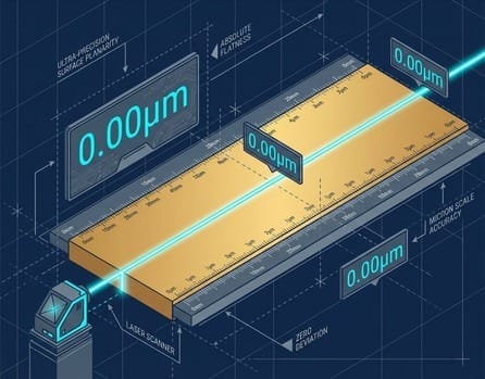
📏 Flatness Anxiety: The Micron-Level Tolerance War
We've been emphasizing "deformation," but why is it so important? Because we're back to the nightmare from the previous chapter—the Pump-out Effect.
If the bottom of the IHS is not sufficiently flat, or if its coplanarity with the chip deviates, then the precious Honeywell PTM7950 layer in between will be uneven in thickness. Thin areas will have good contact, but thick areas (gaps) will experience a sharp increase in thermal resistance. Under a 1000W thermal load, even a gap error of just 0.05mm can cause the temperature in that region to instantly spike by 10°C, leading to "hot spots."
According to the latest industry specifications, NVIDIA's flatness requirements for IHS in the Blackwell generation have reached an almost obsessive "micron (μm) level." This means that every copper lid produced by Kenmec, after high-temperature electroplating and reflow testing, must have surface variations that do not exceed one-tenth the diameter of a human hair.
This explains why the Average Selling Price (ASP) of IHS is experiencing multi-fold growth. This is no longer about selling copper; it's about selling "precision semiconductor components." Only a very limited number of manufacturers can achieve such yield rates, which grants Kenmec extremely strong pricing power and gross margins far exceeding those of the traditional metal processing industry.
🦅 Moat of Trust: One-Stop Surface Treatment
Beyond the manufacturing process, there is another easily overlooked but crucial step: surface treatment.
After IHS fabrication, the surface must be electroplated with nickel (Ni) and gold to prevent oxidation and aid soldering. Controlling the thickness of this plating layer is an art: too thick, and it obstructs heat conduction (nickel has lower thermal conductivity than copper); too thin, and it fails to prevent oxidation. Even more critical, if the electroplating process is not clean, residual chemicals can vaporize at high temperatures, leading to blistering or peeling of the plating layer. Should this occur, the entire packaged GPU would be ruined.
Kenmec possesses its own electroplating facilities and proprietary formulations, enabling it to provide "turnkey" services from forging to electroplating. For TSMC and NVIDIA, this represents the ultimate level of trust. CoWoS capacity is already critically tight, and they would absolutely not risk using a second-tier manufacturer's IHS to save a few dollars.
Kenmec has, in essence, become the most indispensable "metal bodyguard" in this high-stakes CoWoS gamble.
📈 The Curse and Fortune of Area: Non-Linear ASP (Average Selling Price) Explosion
Let's take a look at NVIDIA Blackwell's chip design. Two GPU dies combined with eight HBM3e memory modules lead to a significant increase in the overall package size compared to the previous-generation Hopper (H100).
What does this mean for Kenmec? Many instinctively assume: "If the area doubles, the price of the copper lid should also double, right?" Wrong. In the field of semiconductor precision processing, difficulty and price increase "exponentially."
Geometric Decrease in Yield: When the IHS area is doubled, maintaining "micron-level" flatness over such a large area doesn't just double the difficulty; it increases tenfold. If there's even a slight uneven release of metal stress in the middle, the entire large copper lid will undergo invisible distortion, leading to product scrap. Therefore, globally, fewer than two qualified suppliers can produce such ultra-large IHS. This "extreme scarcity" grants Kenmec absolute pricing power when quoting to chip manufacturers.
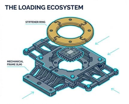
More Than Just a Lid, Also a "Stiffener": According to the latest industry supply chain analysis, the new generation of AI chip cooling solutions is no longer just a copper lid placed on top. To support the massive substrate and prevent it from sagging and cracking due to gravity, the IHS must incorporate complex structures, even combining with a "metal stiffener ring" at the bottom. This means Kenmec is no longer shipping a single component but a "metal kit combination." This directly leads to a quantum leap in the revenue per chip (Content Value).
⚓ ILM (Independent Loading Mechanism): The Underestimated Ecosystem Lock-in Tool
If the IHS is the chip's shield, then the ILM (Independent Loading Mechanism) is the "precision vise" that firmly locks this shield onto the motherboard.
Please do not underestimate this metal frame that presses the CPU/GPU onto the socket. In the AI era, the ILM's strategic importance is shockingly high; it is another high-margin invisible goldmine for Kenmec.
This post is for subscribers only
Sign up now to read the post and get access to the full library of posts for subscribers only.