The 5-2-2 HBM Stacking Crucible: The MR-MUF Crusade and Powertech Technology (6239)'s Sparkling Water Strategy
Analyzing HBM packaging challenges (thermal leakage, high-temp warpage in ultra-thin stacking), contrasting Samsung's precise but inefficient TC-NCF (causing yield bottlenecks) with SK Hynix's breakthrough MR-MUF, a 'holy war' at physical limits crucial for product yield and memory giants' AI-era...
The difficulty of HBM packaging stems from "stacking precision of ultra-thin chips" and "warpage / leakage at high temperatures." The differences in approach between TC-NCF and MR-MUF directly determine yield, production capacity, and thermal dissipation limits.
🍰 Challenging the Laws of Physics: The "Silicon Mille-Feuille" Thinner Than a Human Hair
To understand the complexity of HBM packaging, we must first deconstruct its physical structure.
In the past, memory (DRAM) chips were laid out flat, one by one, on the motherboard. However, AI chips require immense memory capacity while also demanding "extremely short" data transmission distances (because longer distances mean slower speeds and higher power consumption).
Engineers came up with a wild idea: If it won't fit horizontally, let's stack it vertically!
But the thickness of chips is fixed. If eight standard-thickness DRAM chips were stacked together, they would form an obtrusive high-rise tower, unable to fit into a flat server chassis, and a heat sink couldn't be mounted on top.
Consequently, memory manufacturers (such as SK Hynix and Samsung) embarked on an extremely brutal "wafer slimming plan." They had to use chemical and physical grinding methods to drastically thin down the originally robust silicon wafers to a thickness of less than 50 micrometers ($\mu m$)—thinner than a human hair, almost like a translucent cellophane sheet!
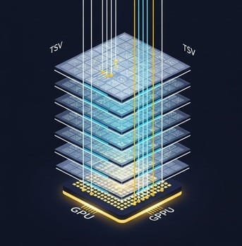
Next, engineers must precisely stack 8, or even 12, layers of these "hair-thin" ultra-thin DRAM chips, much like crafting a "French mille-feuille," layer by excruciating layer.
🏗️ The Micro-Scale Skyscraper's Elevator Shafts and LEGO Bricks
Just stacking them isn't enough; these 12 layers of memory must be able to power each other and communicate with the GPU at the very bottom.
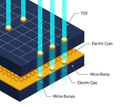
At this point, engineers must drill thousands of extremely tiny vertical deep holes from top to bottom through this cicada-wing-thin mille-feuille. This is the famous TSV (Through-Silicon Via). You can imagine TSVs as the "high-speed elevator shafts" within this 12-story micro-scale skyscraper, responsible for electrons traveling vertically between floors.
After drilling the elevator shafts, the top and bottom surfaces of each chip layer must be embedded with tens of thousands of "micro-bumps," each only a few micrometers in size. When the upper chip layer is pressed down, these micro-bumps must perfectly interlock, like the studs and anti-studs of LEGO bricks, to complete the electrical conduction.
Please visualize this scene:
Imagine 12 sheets of cellophane, thinner than a human hair, stacked together, with thousands of incredibly fine micro-elevators passing through them, and tens of thousands of invisible LEGO-like bumps on each layer that must perfectly align.
This is the true nature of HBM packaging. And once this precise micro-scale skyscraper is built, it awaits the deadly test of high temperatures.
🦑 Two Major Curses of High-Temperature Hell: Leakage and Grilled Squid
When 1600 watts of heat are transferred from the adjacent GPU, HBM faces two physical curses that can instantly render the entire chip defunct:
First Curse: Memory's "Thermal Amnesia" (Leakage)
The operating principle of DRAM relies on extremely tiny capacitors to store electrons (electrons represent 1, no electrons represent 0). This is akin to a series of small cups holding water.
However, when temperatures soar, the vibrations of silicon atoms become extremely violent, and the electrons in these small cups become restless, leading to "leakage." As soon as the temperature exceeds a critical threshold (typically around 85 to 95 degrees Celsius), the electrons storing AI's core weights are instantly lost.
The data painstakingly computed by AI, due to overheating, instantly "loses its memory."
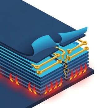
Second Curse: Mille-Feuille Collapse (Warpage)
This is the ultimate nightmare for packaging engineers.
All materials expand and contract with temperature changes. When these 12 layers of silicon chips, thinner than a human hair, encounter high temperatures, they begin to deform dramatically due to uneven heating.
This is like placing a thin piece of raw squid on a hot grill—the edges of the squid instantly curl up!
This phenomenon in the semiconductor industry is known as "warpage."
If even one layer among these 12 mille-feuille layers has its edge slightly curl upwards by just one micrometer ($\mu m$) due to heat, the "micro-bumps" (LEGO bricks) on that layer will be mercilessly torn apart. Once a connection breaks, the entire 12-layer HBM micro-scale skyscraper is declared dead.
⚔️ The Zero-Tolerance Battlefield
This is why we refer to HBM packaging as a "battlefield."
In traditional chip manufacturing, if one chip fails, you simply discard it.
However, in the world of HBM, you are stacking 12 perfectly fabricated, extremely expensive DRAM chips together. In the final packaging stage, if it's even slightly misaligned by one micrometer, if just one micro-bump isn't properly connected, or if it succumbs to high temperatures and warps...
All 12 chips in the "entire stack" will be scrapped together. You don't just lose the cost of one chip; you lose the full cost of 12 top-tier chips plus the highly expensive packaging process!
Yield, here, is not just a financial figure; it is the gateway to life or death for memory manufacturers.
👔 Samsung's "Iron and Cling Film": The Precise Yet Fatal TC-NCF Process
As the long-standing absolute hegemon in global memory, Samsung initially faced the HBM stacking challenge by choosing a technical route that seemed the most secure and aligned with traditional engineering intuition—TC-NCF (Thermal Compression - Non-Conductive Film).
To understand this technology, please imagine a highly relatable scene in your mind: "Using a hot iron, press 12 pieces of clothing together, one by one, with double-sided tape in between."
In Samsung's cleanroom, the actual TC-NCF operation proceeds as follows:
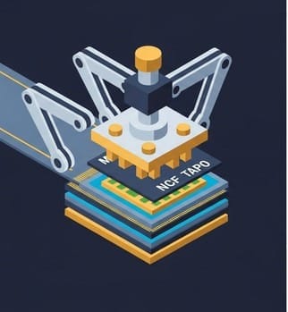
Laying the film (double-sided tape): A robotic arm first lays a solid insulating film called NCF (like an extremely precise double-sided tape) on the bottom chip.
Placing the chip: Next, the second DRAM chip, thinner than a human hair, is precisely stacked on top.
High-temperature thermal compression (iron): Subsequently, an ultra-precise equipment called TCB (Thermal Compression Bonder) presses down heavily from directly above, like a "hot iron." The high temperature instantly melts the micro-bumps (metal contacts) beneath the chip, and the immense pressure firmly squeezes the NCF film into every tiny gap, bonding the two chip layers tightly together.
Cooling and repeating: After pressing, it's allowed to cool and solidify. Then, another film is laid, a third layer is stacked, and the iron presses again... This process is repeated 12 times.
Advantages of TC-NCF: Ultimate Thickness Control
Samsung chose this path for a reason. Because the force and temperature of each press by the TCB iron can be precisely controlled, and the thickness of the NCF solid film is fixed. This allows Samsung to perfectly control the final height of this 12-layer micro-scale skyscraper, ensuring identical spacing between each layer and preventing tilting.
Fatal Physical Flaws: Thermal Hell and Glacially Slow Production
However, as HBM entered the AI era, facing terrifying heat loads of up to thousands of watts from NVIDIA GPUs, Samsung's TC-NCF approach hit two fatal physical walls:
First Wall: The "Heat Trap" of Cling Film. NCF film is essentially a polymeric plastic material. Plastic does not conduct heat! This means Samsung forcibly inserted 12 layers of "non-heat-dissipating cling film blankets" between these 12 layers of fiercely heat-generating chips. Heat is firmly trapped in the core of the mille-feuille and simply cannot dissipate. This directly triggered the "thermal amnesia (leakage)" we mentioned earlier, causing HBM to frequently crash during high-temperature operation.
Second Wall: Despairingly Slow Production Speed. Imagine: each layer requires one press from the iron, waiting for it to melt, then waiting for it to cool. 12 layers mean repeating 12 cycles of heating and cooling. This not only makes production glacially slow, but more alarmingly, after enduring 12 cycles of "thermal expansion and contraction," the chip edges are very prone to "warpage," leading to contact breakage.
This is the underlying reason why Samsung's yield in the HBM3 and HBM3E generations has consistently struggled painfully between 40% and 50%. It's not that Samsung isn't trying; it's that this physical approach is inherently unsuitable for the extreme high-temperature AI battlefield.
🍰 SK Hynix's "Oven and Potting Magic": The Industry-Shocking MR-MUF
While Samsung struggled in the quagmire of irons and films, SK Hynix, long the second-largest player, demonstrated the strategic determination to burn its bridges. They completely abandoned traditional film thermal compression methods and invented a packaging divine technique that can only be described as "magic"—MR-MUF (Mass Reflow - Molded Underfill).
The metaphor for this technology is quite wild: "Stacking 12 layers of cake all at once, baking them directly in an oven, and then, once removed, simultaneously injecting heat-conductive liquid syrup perfectly into every tiny gap between the layers."
Let's deconstruct this "black technology" that Jensen Huang can't get enough of:
Phase One: MR (Mass Reflow)
SK Hynix engineers no longer iron layer by layer. They directly stack all 12 chips, coated with a special flux, precisely into a tower. Then, without applying pressure with any iron, this entire 12-layer tower is sent "all at once" into a giant high-temperature oven (Reflow Oven) with precise temperature control. Inside the oven, tens of thousands of micro-bumps between the 12 layers of chips instantly melt and perfectly solder at the same time!
Advantages: Extremely fast! Others iron 12 times; SK Hynix only bakes once. And because of even heating, it significantly reduces warpage issues caused by repeated thermal expansion and contraction.
Phase Two: MUF (Molded Underfill)
This is the "absolute secret" that allowed SK Hynix to pull ahead of Samsung. After being removed from the oven, there are still gaps between the 12 chip layers. At this point, SK Hynix's machines use extremely precise pressure to instantly inject a "special liquid epoxy resin" into all the gaps of this 12-story building, tightly encapsulating the entire structure.
This liquid adhesive is not ordinary glue. It is a "thermal dissipation miracle adhesive" whose formula is classified as a top trade secret, developed by SK Hynix and top Japanese chemical manufacturers (such as Namics) over several years. Within this transparent liquid adhesive, countless nano-sized "highly conductive particles (usually aluminum oxide or aluminum nitride)" are suspended.
When this liquid adhesive flows into the chip gaps and cools to harden, it transforms into an incredibly hard solid block with "extremely high thermal conductivity."
The Physical Miracles Created by MR-MUF:
Perfect Thermal Dissipation Channels: The nano-sized conductive particles create countless microscopic thermal dissipation bridges between the chips. The high temperature transferred from the GPU can instantly and smoothly be guided out of the chip through these hardened adhesive bodies. Thermal dissipation efficiency is several times higher than Samsung's NCF plastic film!
Ironclad Structural Strength: The hardened MUF adhesive acts like high-strength reinforced concrete poured into this 12-story building. The chips are firmly held within the solid adhesive, ensuring that they "absolutely cannot warp (Zero Warpage)," no matter how high the temperature.
This is SK Hynix's ultimate trump card that allowed it to exclusively secure NVIDIA H100 and B200 as the primary HBM suppliers. Their MR-MUF process perfectly solved the most fatal high-temperature and warpage curses of AI chips!
📊 The Cruel Verdict of Foreign Investment Data: The FCF Money Printer and the "Struggling Giant"
This post is for subscribers only
Sign up now to read the post and get access to the full library of posts for subscribers only.