📐 The Cruelty of Geometry: The 'Round Table Trap' of 12-inch Wafers
The starting point of this cross-industry massacre stems from a simple elementary school geometry problem: "Chips are square, but wafers are round."
In traditional Fan-Out Wafer Level Packaging (FOWLP, such as TSMC's InFO), engineers arrange diced chips onto a 12-inch (300mm diameter) "round" carrier for packaging.
Imagine trying to fit as many "square" bento boxes as possible onto a "round table". What happens?
No matter how meticulously you arrange them, there will always be unfilled curved gaps along the "edges" of the round table.
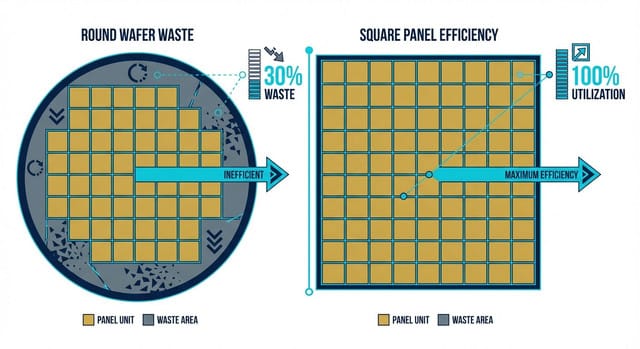
In semiconductor manufacturing, this is known as Edge Loss. According to industry statistics, arranging square chips on a 12-inch round wafer always wastes as much as 15% to 20% of the area!
And this doesn't even account for the inherent area ceiling of 12-inch wafers. If chips continue to grow larger, the total number of chips that can be cut from a single 12-inch wafer decreases, naturally keeping the per-chip packaging cost prohibitively high.
⬛ The Crushing Force of Squares: FOPLP's Area Magic
To solve this geometric conundrum, the industry proposed FOPLP (Fan-Out Panel Level Packaging).
Its core logic is simple and straightforward: Since chips are square, why don't we switch the packaging substrate to "square" as well!
FOPLP completely abandons 12-inch round wafers, opting instead for square glass or metal panels as carriers, with sizes up to 510mm x 515mm or even 700mm x 700mm.
This is no laughing matter when it comes to area advantage:
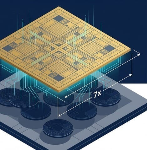
- Sevenfold Capacity Boost: A 700mm x 700mm square panel offers an available surface area more than 7 times that of a traditional 12-inch wafer!
- Near-Zero Edge Loss: Arranging square chips on a square panel is like arranging bento boxes on a square table—you can fit them perfectly, achieving an area utilization rate of over 95%.
This means that for each packaging run, FOPLP produces several times more chips than traditional FOWLP. In the semiconductor industry, which emphasizes economies of scale, this effectively slashes manufacturing costs for packaging (industry estimates suggest a reduction of 30% to 50%).
♻️ Innolux (3481)'s Tears and the "Alchemy of Scrap"
If FOPLP is so advantageous, why didn't traditional outsourced semiconductor assembly and test (OSAT) companies (such as ASE Technology Holding, Siliconware Precision Industries) switch entirely to square panels sooner?
The answer is: equipment incompatibility! The billions of US dollars spent by traditional semiconductor manufacturers on machines, robotic arms, and conveyor tracks were all designed for "300mm diameter circles." To switch to large square panels, all equipment in the entire fab would have to be "scrapped and rebuilt," representing an astronomical capital expenditure (Capex).
But then, a cross-industry assassin with "free fabs" arrived: Innolux (3481), Taiwan's major panel manufacturer.
In recent years, panel manufacturers in Taiwan have shed many bitter tears under the fierce competition from China's "red supply chain." They possess numerous older generation (3.5-gen, 4.5-gen) LCD panel fabs that, unable to produce competitive TV or mobile phone screens, had almost become economically worthless scrap.
However, in the FOPLP battle, these "scraps" suddenly became invaluable treasures!
Because the original work of panel manufacturers involves "daily micrometer-level processing on extremely large square glass!"
Innolux realized with a start: Even though my 3.5-generation line is losing money making panels, if I refit it for FOPLP packaging, it would be a dimensional attack!
Even more remarkably, depreciation for Innolux's old fab equipment had already been fully amortized years ago!
While traditional OSAT giants are still meticulously calculating the massive depreciation costs of purchasing brand-new square equipment, Innolux is essentially entering the packaging market with "zero-depreciation, free fabs and machinery" to wage a price war. This is an "alchemy of scrap" that only panel manufacturers can afford to play.
🎯 Debunking Myths: FOPLP Is NOT for NVIDIA B200!
When many retail investors in the market hear the term "panel-level packaging," they often excitedly assume that Innolux is preparing to package NVIDIA's highest-end AI chips.
This is an extremely dangerous misconception.
In advanced packaging specifications, there is a key metric called L/S (Line/Space, line width and spacing).
- TSMC's CoWoS has an L/S scaled down to below 1 micrometer (even advancing towards 0.4 micrometers), which is necessary for top-tier beasts like H100 and B200, which contain hundreds of billions of transistors.
- However, current FOPLP (panel-level packaging), limited by the physical properties of glass substrates and the precision of existing equipment, can only achieve an L/S of approximately 2 to 5 micrometers.
This means that Innolux's square panels "absolutely cannot produce" the top-tier AI chips at present.
But Innolux has no intention of competing for TSMC's high-end business! Innolux's strategy is very shrewd: "I want to capture the 'underserved market'—that 99% that TSMC disdains and traditional OSAT companies find insufficiently profitable!"
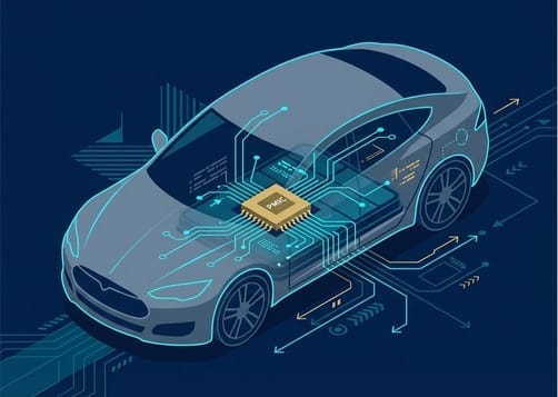
🚗 The Anxiety of European Giants: Why NXP?
In this vast underserved market, the most anxious and cost-sensitive players are the giants in "automotive chips" and "power management integrated circuits (PMIC)." European automotive semiconductor leader NXP is a prime example, and also Innolux's most emblematic heavy-weight client for FOPLP.
Why is NXP willing to entrust its chips to Innolux? Let's analyze the two critical pain points of automotive chips:
1. No need for 5nm, 28nm is more than sufficient:
Automotive chips (such as microcontrollers or MCUs for controlling car windows, brakes, and power management) prioritize "absolute reliability in extreme environments" over computational speed. Therefore, most of them use mature processes like 28nm or 40nm. These chips have relatively coarse line widths, and their packaging L/S precision requirements are typically in the micrometer range.
This falls perfectly within FOPLP's "optimal range"!
2. Enormous volume and extreme "cost sensitivity":
A modern electric vehicle (EV) might contain thousands of power management ICs (PMICs) and sensor chips. While the unit price of these chips is not high, their usage volume is enormous. For NXP, if traditional 12-inch wafer-level packaging (FOWLP) costs $10, they would dream of cutting that cost in half.
🔪 The Ultimate Allure of Drastic Cost Reduction
At this point, Innolux presented its massive 700mm x 700mm square glass panel.
Innolux told NXP: "With traditional 12-inch round wafers, 15% of the space is always wasted at the edges. Now, I can arrange your automotive chips densely, like bento boxes, on my large square table. My production line runs once, producing seven times the number of chips compared to traditional packaging. Furthermore, the equipment depreciation for my 3.5-generation fab has already been fully amortized, meaning I'm essentially providing manufacturing services using a free fab."
Under the combined assault of "area advantage" and "zero-depreciation fabs," the industry estimates that FOPLP can directly slash the packaging cost of such chips by 30% to 50%!
For automotive and consumer electronics giants who meticulously scrutinize gross margins, such a significant cost reduction is simply irresistible. This is the fundamental reason why NXP is willing to take on cross-industry risks and collaborate with Innolux to adopt panel-level packaging for its PMIC chips.
With this inexpensive square table, Innolux precisely targeted the soft underbelly of traditional OSAT companies, officially tearing open a bloody breach in the semiconductor landscape.
⚔️ The FOPLP Three Kingdoms Saga: A Contest of Cost, Technology, and Hegemony
In the current FOPLP battleground in Taiwan, three distinct, massive forces with entirely different strategic logics have emerged. To understand who will prevail, we must first understand the cards they hold:
1. Innolux (3481)'s 'Cost-Driven Approach': The Wildly Growing Disruptor
Innolux's biggest moat is its "zero-depreciation old fabs" and extensive experience in "processing ultra-large glass," which we mentioned earlier. They are waging a pure price war, crushing competitors with sheer area advantage.
But Innolux's fatal flaw is: they don't understand semiconductors.
Drawing circuits on a glass screen versus drawing circuits on micrometer-scale silicon chips are two entirely different worlds in terms of yield standards. Innolux's biggest challenge now is how to overcome the bottomless "yield learning curve" of semiconductors.
2. Powertech Technology (6239)'s 'Technology-Driven Approach': The Solitary Pioneer
Compared to Innolux's late entry, Powertech Technology, Taiwan's leading memory OSAT company, is a pure OSAT player that has quietly pioneered in the FOPLP field for over six years.
Powertech Technology does not pursue a low-price dumping strategy; instead, they aim for "high-quality panel-level packaging." They deeply understand that precisely controlling stress and material warpage on large square panels requires an extremely profound patent portfolio. Powertech Technology currently holds the most comprehensive FOPLP process patents and is the frontrunner with the highest technological maturity. For IC design companies that demand extremely high quality while also seeking cost reduction, Powertech Technology is a more reassuring choice than a panel manufacturer.
3. ASE Technology Holding (3711)'s 'Client-Driven Approach': The Opportunistic Apex Predator
Many people wonder: if FOPLP has so much potential, why does ASE Technology Holding, the global OSAT leader, seem so calm and slow-paced?
This is the confidence of a hegemon. ASE Technology Holding knows that the current FOPLP landscape is in a "Warring States period," where panel sizes are not unified (some use 510x515mm, others 700x700mm), and equipment specifications are highly chaotic.
ASE Technology Holding's strategy is to "let the bullets fly for a while." They hold the largest number of top-tier clients globally. Once Innolux and Powertech Technology have refined equipment specifications and market standards are established, ASE Technology Holding can, at any time, leverage its vast capital to directly acquire the most advanced equipment, or even directly acquire relevant competitors, harvesting the entire market with a late-mover advantage.
🧊 The Think Tank's Cold Insight: Piercing Innolux's Short-Term EPS Fantasy
After analyzing the Three Kingdoms saga, we must now provide the most brutal reality check against the market's frenzy surrounding "panel manufacturers crossing over."
Based on our think tank's in-depth exploration of underlying technological pathways and internalized analysis of capital flows within the global top-tier supply chain, we must point out a technical truth that the market has deliberately ignored: the vast chasm between "Chip-First" (chip-first bonding) and "Advanced Packaging."
Currently, Innolux's FOPLP technology primarily remains at the relatively early Chip-First (bonding chips before wiring) stage. This technique is relatively simple and highly suitable for producing the legacy ICs (such as mature process automotive chips or PMICs) we mentioned earlier.
However, if the goal is to move towards higher-end computing chips in the future, it is essential to switch to the extremely difficult RDL-First (creating the redistribution layer first, then bonding chips). Doing RDL-First on a massive 700mm panel means that even slight temperature variations will cause micrometer-scale lines across the entire glass to shift, leading to misalignment when chips are bonded and rendering the entire panel scrap.
This is an extremely cruel technological chasm.
Therefore, we arrive at an extremely rational and crucial strategic conclusion:
- High-end applications remain out of reach: Innolux's current technological capabilities are a very long way from true "Advanced Packaging." Expecting them to secure high-end AI computing chip orders in the short term is an extremely unrealistic fantasy.
- Substantial financial contribution is extremely low: Even if Innolux begins small-volume shipments of automotive and mature ICs by mid-2025, compared to their immensely large "traditional commodity panel" revenue (which is still projected to account for about 45% of their total revenue in 2026), FOPLP's actual revenue and profit contribution to Innolux's overall performance between 2026 and 2027 will be "very, very limited (Limited Contribution)."
FOPLP is absolutely a great lifeline for Innolux to escape the panel industry's cyclical downturns and drive corporate transformation. They have acquired automotive-related companies (such as Pioneer) and are steadily building their long-term automotive portfolio.
But please remember, this is a fundamental strategic transformation that will take five to ten years, not a short-term panacea that will make EPS surge in the next quarter. Blindly chasing up its valuation now because of the FOPLP theme will incur significant time costs and technology ramp-up risks.
🚪 A Perfect Transition: The Iron Rule of a Gold Rush—Who's Selling the Square Shovels?
The final wave of the 5-3-2 analysis concludes here.
After reading this highly rational analysis, you might feel a touch of disappointment: "Since Innolux won't be making big money in the short term, Powertech Technology is still pioneering technology, and ASE Technology Holding is still observing, then who precisely reaped the first massive profits from this widespread FOPLP fab construction boom?"
Recall the 19th-century California Gold Rush in the United States.
Before the actual gold veins were even discovered, those hopeful prospectors were burning through their money. The ones truly counting stacks of cash and making a fortune were those "selling shovels and denim jeans" by the roadside!
The current FOPLP situation perfectly reenacts this historical iron rule.
Please consider a physical fact: traditional semiconductor factory equipment, whether conveyor tracks, vacuum chucks, or ovens, were all designed for "300mm diameter round wafers."
Now, Innolux and Powertech Technology suddenly introduce a massive 700mm x 700mm "square glass" panel.
This means that all equipment on the entire production line, from start to finish, inside and out, will have to be "scrapped and rebuilt"!
Traditional foreign semiconductor equipment giants (such as Applied Materials, ASML) are completely bewildered by this large square table, as they have never built such large square machines.
However, Taiwan has a group of "invisible champions" who, for the past thirty years, have dealt with massive "square PCB circuit boards" and "square LCD panels" every single day.
For them, FOPLP is not a challenge at all; this is an "absolute home turf" where they can win with their eyes closed!
In-depth Research · Quantitative Perspective
Want more quantitative research insights on semiconductors?
【Insight Subscription Plan】Break Free from Retail Investor Mentality: Build Your Alpha Trading System with "Quantitative Chips" and "Consensus Data"EDGE Semiconductor Research
📍 Series Map — Navigate the Complete EDGE Semiconductor Research →


