When we discuss AI infrastructure, the most frequently heard term is "compute power"; however, for data center architects, the true persistent nightmare is the "Power Wall."
At 1.6T (1600G) speeds, pluggable optical modules' total power consumption will account for over 50% of an entire switch's energy consumption. To break this vicious cycle, we must "remove" optical modules from the switch's faceplate and move them directly into the switch chip (ASIC) package. This is the essence of CPO technology: eliminating the long-distance PCB traces that attenuate signals and generate heat from electrons.
🛡️ Chapter One: Broadcom's Bailly Platform — CPO's Commercialization Pioneer
If CPO is the holy grail of optical communications, then Broadcom is the first arms dealer to bring that holy grail to customers.
1. The 51.2T Physical Leap: The Arrival of the Bailly Chip
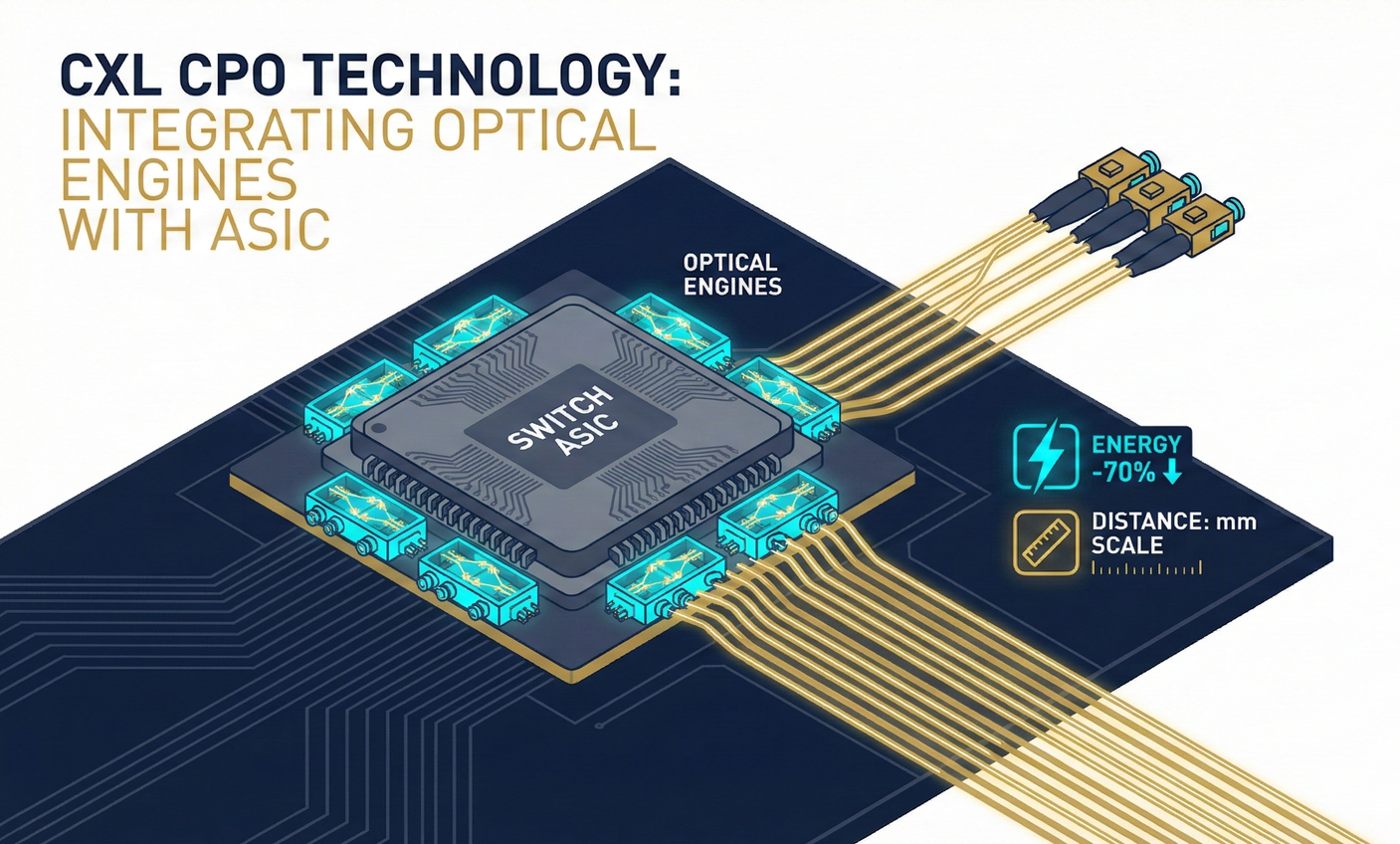
As early as March 2024, Broadcom announced that its Bailly 51.2T CPO switch officially entered commercial production. This is not just a chip, but a massive "System-in-Package (SiP)":
- Integration of 8 Optical Engines: Within the Tomahawk 5 ASIC package, Broadcom directly integrated 8 silicon photonics engines, each with 6.4Tbps bandwidth.
- Elimination of Retimer Requirement: Because the distance between the optical engine and the chip has shrunk from "centimeter-level" to "millimeter-level," signal attenuation is almost nonexistent, thus eliminating the need for extremely power-intensive DSP or Retimer chips.
2. Formidable Energy Efficiency: 70% Power Savings
According to official Broadcom data and industry test results, the Bailly platform achieves the following breakthroughs compared to traditional pluggable modules:
- Dramatic Power Drop: Transmission power consumption plummets from 15 picojoules per bit (pJ/bit) for pluggable modules to 5 picojoules, achieving energy savings of up to 70%.
- Doubled Density: Panel space is no longer occupied by bulky OSFP modules, allowing data centers to pack double the compute power into the same rack space.
3. The Next Stop in 2026: 102.4T and 200G SerDes
Entering 2026, Broadcom is accelerating its progress towards a 102.4T CPO platform based on Tomahawk 6. This system will fully adopt 200G/lane technology, meaning CPO will no longer be merely a "laboratory luxury," but the "only viable path" for hyperscale clusters in the 1.6T era.
🛰️ Chapter Two: Google's All-Optical Path Ambition — Why a Software Giant is Pushing Hard on Hardware?
You might ask why Google's depth of involvement in hardware architecture far surpasses all companies except NVIDIA. The answer lies in Google's self-developed AI chip — the TPU (Tensor Processing Unit).
1. The "Energy-Saving Obsession" of TPU Clusters
Google anticipates deploying over 5 million TPUs by 2027. At this scale, if traditional electrical connection schemes were to continue, the power consumed solely by "communication" would be enough to cripple Google's entire capital expenditure. Therefore, Google has become the most aggressive proponent of CPO technology.
- Optical-Electrical Integration: Google's goal is to integrate optical interfaces directly into TPU v7 (Ironwood) or future versions, allowing optical signals to travel directly from the chip's core across racks.
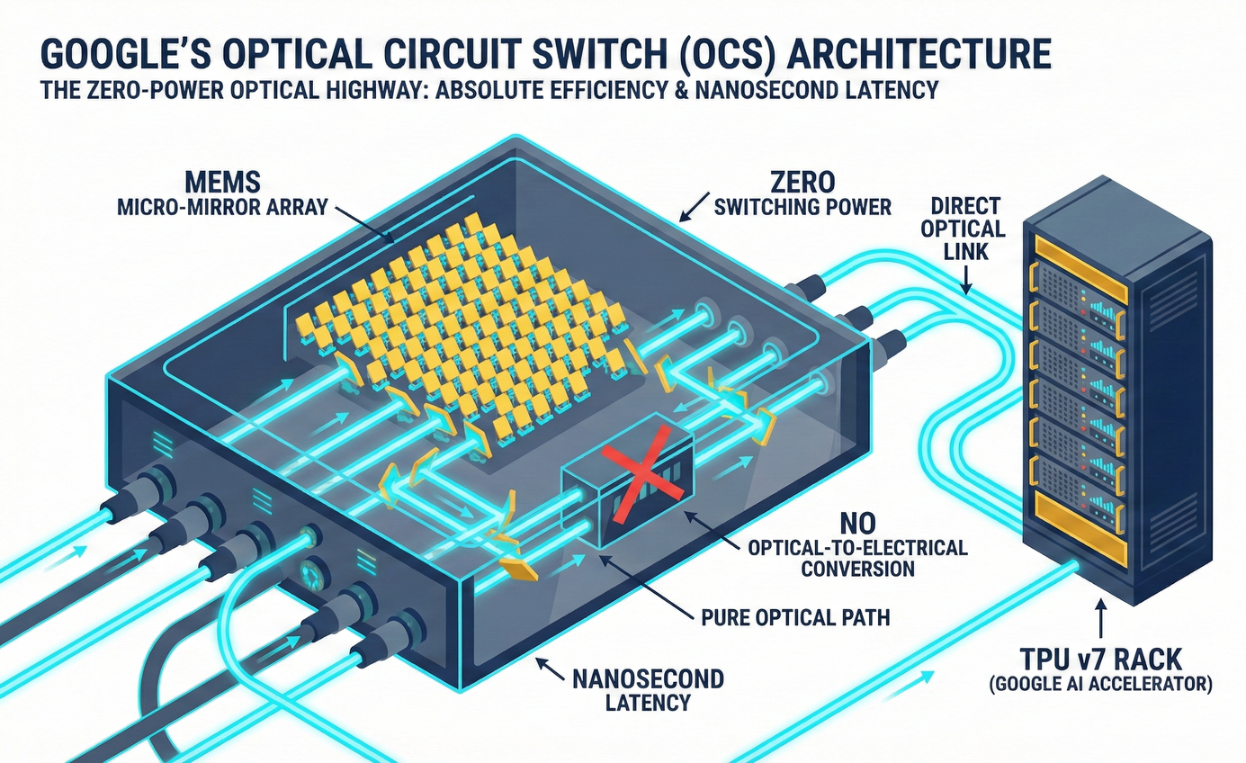
2. The Divine Assist from Apollo OCS (All-Optical Switching Technology)
Google's strong push for CPO is underpinned by its globally unique Apollo OCS (Optical Circuit Switch) technology.
- Micro-Mirrors (MEMS): This system uses tiny mirrors to reflect light, completely bypassing the "optical-to-electrical" conversion process. This provides Google's data center network with extremely low latency and near-zero power consumption switching capabilities.
- The Ultimate Combination of CPO + OCS: When photons generated by TPUs directly enter the OCS switching matrix, Google can build the world's most energy-efficient AI supercomputers.
🔪 Chapter Three: Silicon Photonics' Cost Carnage — Why CMOS Will Win?
In 4-3-1, we discussed the contention between EML (traditional aristocracy) and silicon photonics (commoner revolution). In the CPO era, this is no longer just about technical merits, but a brutal economic strangulation.
1. The Ultimate Principle of Economies of Scale
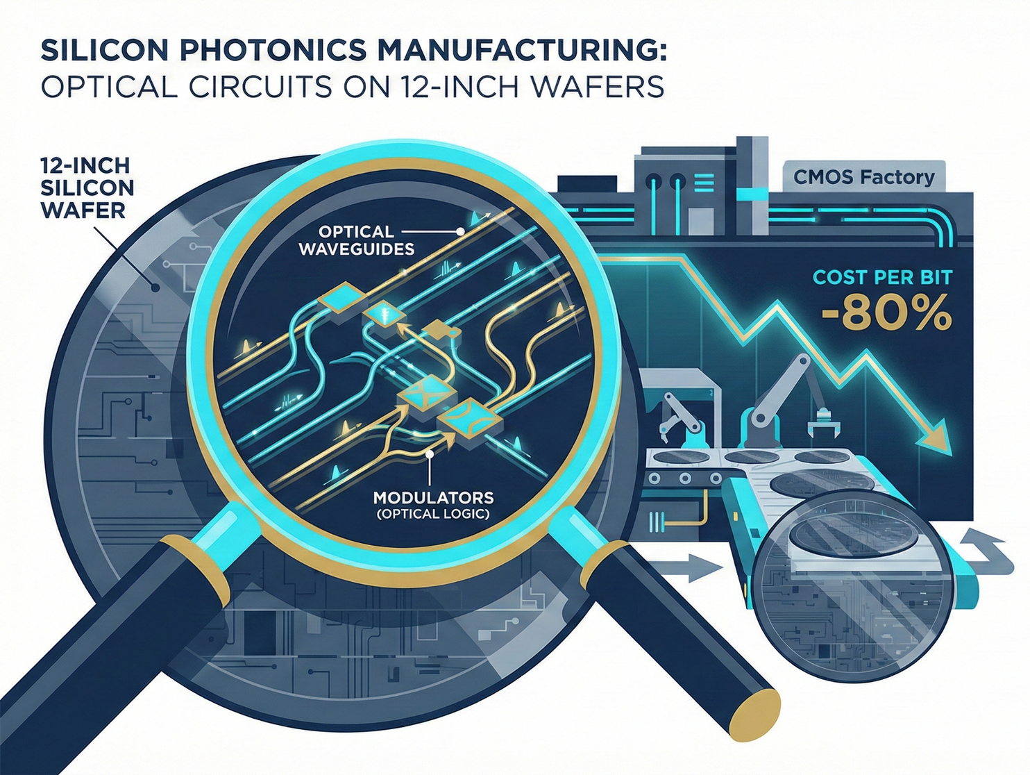
Traditional EML lasers require expensive Indium Phosphide (InP) material and must be produced in specialized compound semiconductor wafer fabs, leading to slow capacity expansion and high unit costs.
- Silicon Photonics' "Moore's Law": Silicon photonics technology etches optical components (modulators, waveguides, etc.) directly onto 8-inch or 12-inch silicon wafers. This means it can leverage the extremely mature CMOS process of leading foundries like TSMC for mass production.
- Cost Scissors Gap: When speeds reach 1.6T and above, the per-bit cost of silicon photonics solutions will create a significant "scissors gap" compared to traditional EML. The higher the volume, the lower the average cost of silicon photonics, which is devastating for traditional laser manufacturers relying on high-margin, small-scale production.
2. Qualitative Change in Integration
Silicon photonics can "miniaturize" hundreds of optical components into a single chip. Under the CPO architecture, Broadcom's Bailly platform can pack up to 102.4T of total bandwidth into an extremely small space. This level of integration is a physical limit that traditional optical modules, assembled manually or semi-automatically, simply cannot achieve.
⚰️ Chapter Four: The 2028 Deadline — Optical Module Manufacturers' Identity Crisis
This CPO revolution is creating an "identity crisis" for today's thriving optical module giants. If optical modules are "eliminated" in the future, directly soldered next to switch chips, where do today's module manufacturers go?
1. From "Box Manufacturer" to "Packaging Foundry"
When pluggable modules are replaced by CPO, the optical module manufacturers' original "black boxes" will cease to exist.
- Transformation Path: The future viability for module manufacturers lies in transforming their accumulated optical alignment and testing capabilities into providing SiP (System-in-Package) foundry services for CPO engines.
- Technology Gap: 2026 to 2028 will be a critical transition period. Only manufacturers with silicon photonics design capabilities and automated alignment equipment will remain on Tim Cook's or Jensen Huang's shortlist.
2. 2028: CPO's Commercialization Watershed
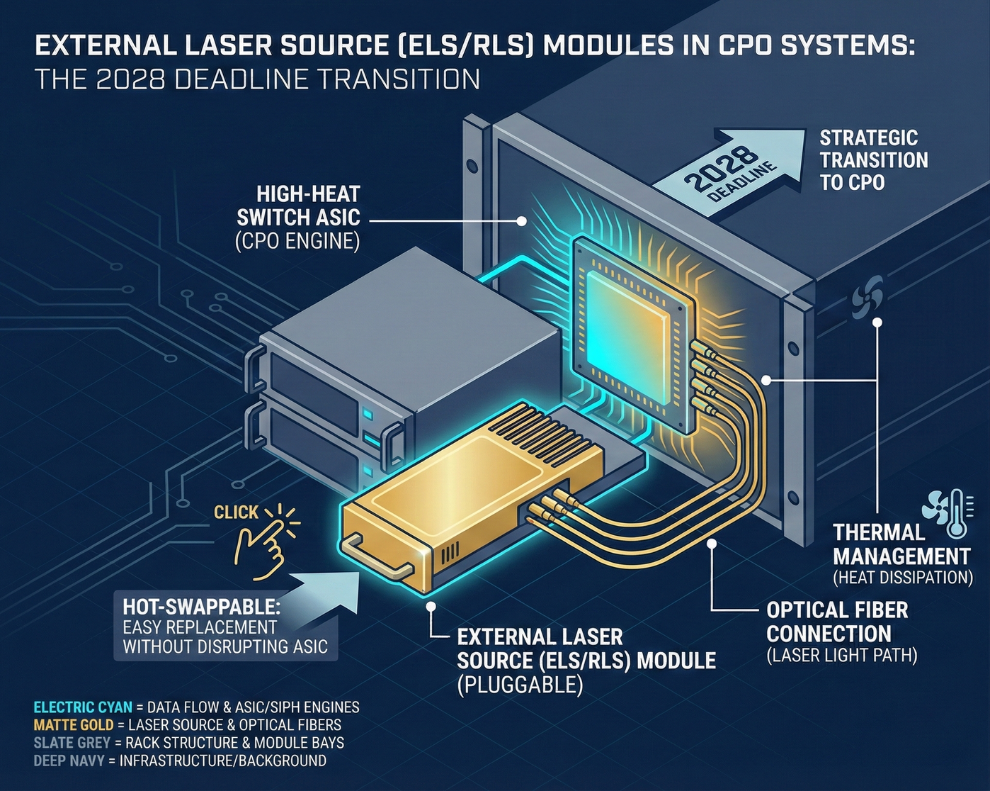
According to Google and Broadcom's deployment timelines, CPO is expected to reach the critical point of mass commercialization in 2028.
- Standardization War: Currently, CPO's biggest pain point is "difficulty of repair" — if a laser fails, must the entire expensive CPU be replaced?
- The Turning Point for Remote Laser: To mitigate risks, the industry is promoting moving the laser source externally (RLS). This leaves traditional laser manufacturers (such as Lumentum) with their last "strategic high ground": becoming professional high-power remote light source suppliers.
📊 4-3-4 Strategic Summary: Google and Broadcom's "All-Optical Path" Game
Let's summarize the core insights of 4-3-4:
- Google's objective is not just to save money: It's to break through the "Power Wall" and prevent its computing clusters, composed of millions of TPUs, from collapsing due to communication overheating.
- Broadcom's Bailly is a dimension-reducing strike: Through deep integration of silicon photonics and ASICs, Broadcom is "vertically compressing" the optical communication industry chain, shifting it from a component market to a packaging system market.
- Silicon photonics is the only physical path to survival: As single-channel rates move towards 224G and even higher, silicon photonics, leveraging its cost and integration advantages in CMOS processes, will become the dominant technology after the 1.6T era.
In-depth Research · Quantitative Perspective
Want more semiconductor quantitative research insights?
【Insight Subscription Plan】Break Free from Retail Investor Mentality: Build Your Alpha Trading System with "Quantitative Chips" and "Consensus Data"EDGE Semiconductor Research
📍 Series Map — Navigate the Complete EDGE Semiconductor Research →


