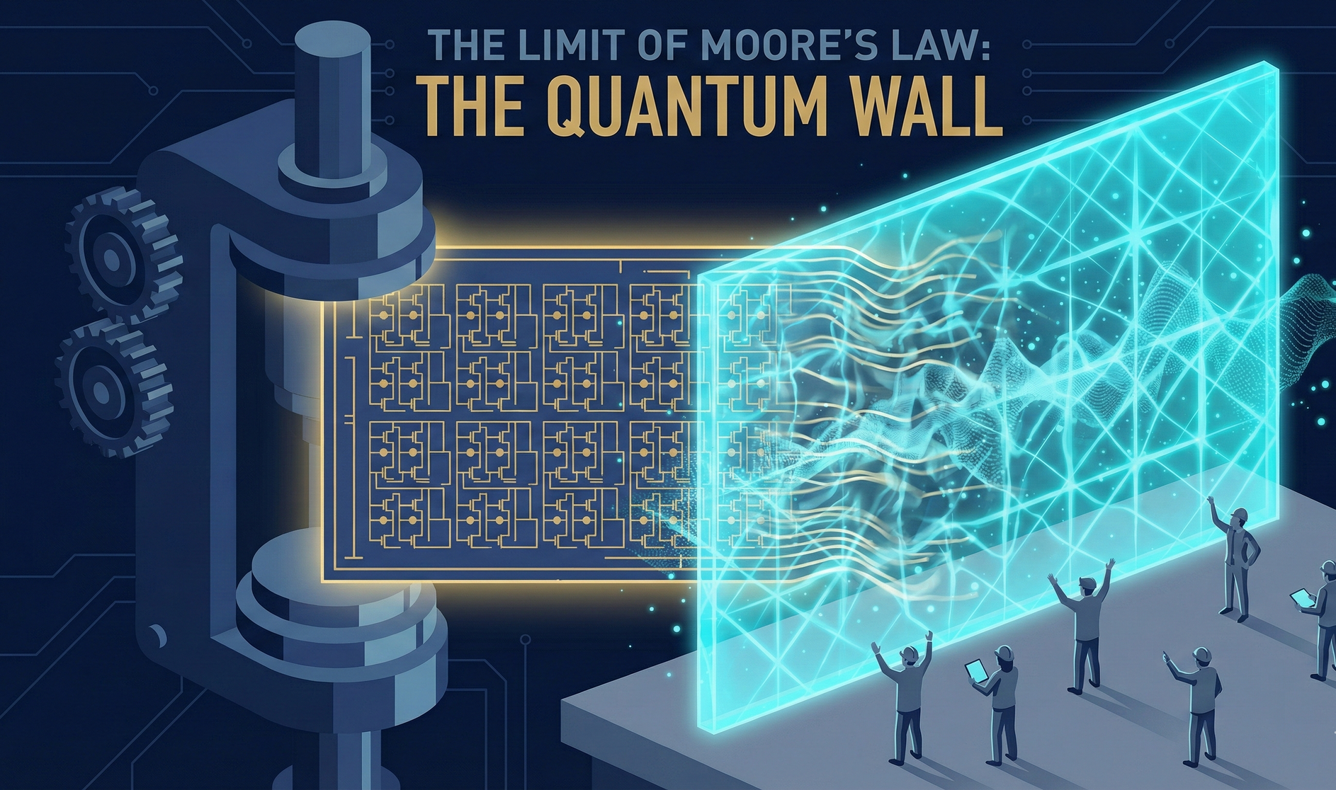
Before diving into this "architectural holy war" that will determine the technological supremacy of the next decade, we must first pause and look back at the path we have traveled.
In the previous chapters of the 2-5 series, we carefully examined the "microcosmic cycle of reincarnation" of semiconductor manufacturing as if under a magnifying glass. We witnessed how ASML's Extreme Ultraviolet (EUV) lithography, like a divine hand, etched extremely fine lines of tens of nanometers onto wafers; we saw how Applied Materials and Lam Research's plasma etchers precisely dug deep trenches with atomic accuracy; and we understood how KLA's electronic eyes precisely pinpointed that one fatal speck of dust in an ocean of detail.
This was an era dominated by "god-tier tools." For the past thirty years, the logic of wafer manufacturing was surprisingly simple and crude: as long as you had sufficient capital to acquire the latest and most expensive equipment, you could dominate Moore's Law.
But now, as engineers at TSMC, Intel, and Samsung push process technology deeper into the territory of 3 nanometers (3nm) and even approaching 2 nanometers (N2), they look at the world's most powerful machines in the cleanroom, costing hundreds of millions of dollars and representing the pinnacle of human industrial achievement, and a deep sense of despair rises within them.
Why? Because a harsh truth stands before them: the problem is no longer with the "tools"; the problem lies with the "blueprint" itself.
1. The Vanishing Free Lunch: The Death of Dennard Scaling
To understand the panic faced by foundries today, we must first understand how fortunate they once were.
From the 1970s to the early 2000s, the semiconductor industry operated under a golden rule even more wondrous than Moore's Law: Dennard Scaling. This law presented engineers with a wonderful fairy tale: when you shrink a transistor's size by half, you could not only pack twice as many transistors onto the same chip area, but also, it would run faster and consume less power!
Commercially, this was an incredible "free lunch." You made things smaller, and not only did performance double, but costs also decreased. In that golden era, the strategies of TSMC and Intel were exceedingly simple: shrink, shrink, and shrink again. All they had to do was call ASML for a higher-resolution lithography machine, contact chemical manufacturers for better photoresists, and scale down the 2D planar blueprint, and the next generation of "god-tier" chips would naturally emerge. Everything was so self-evident.
However, around 2005, as transistor gate lengths shrank to 65 nanometers and continued to approach 20 nanometers, this free lunch was abruptly taken away. Engineers were alarmed to discover that while chips continued to get smaller, they were no longer power-efficient; instead, they began to generate immense heat.
This was the famous "Thermal Wall" crisis. Why did this happen? Because we hit the boundaries of classical physics, awakening the ghosts of the microscopic world.
2. Hitting the Physical Wall: Encountering the Ghost of Quantum Mechanics
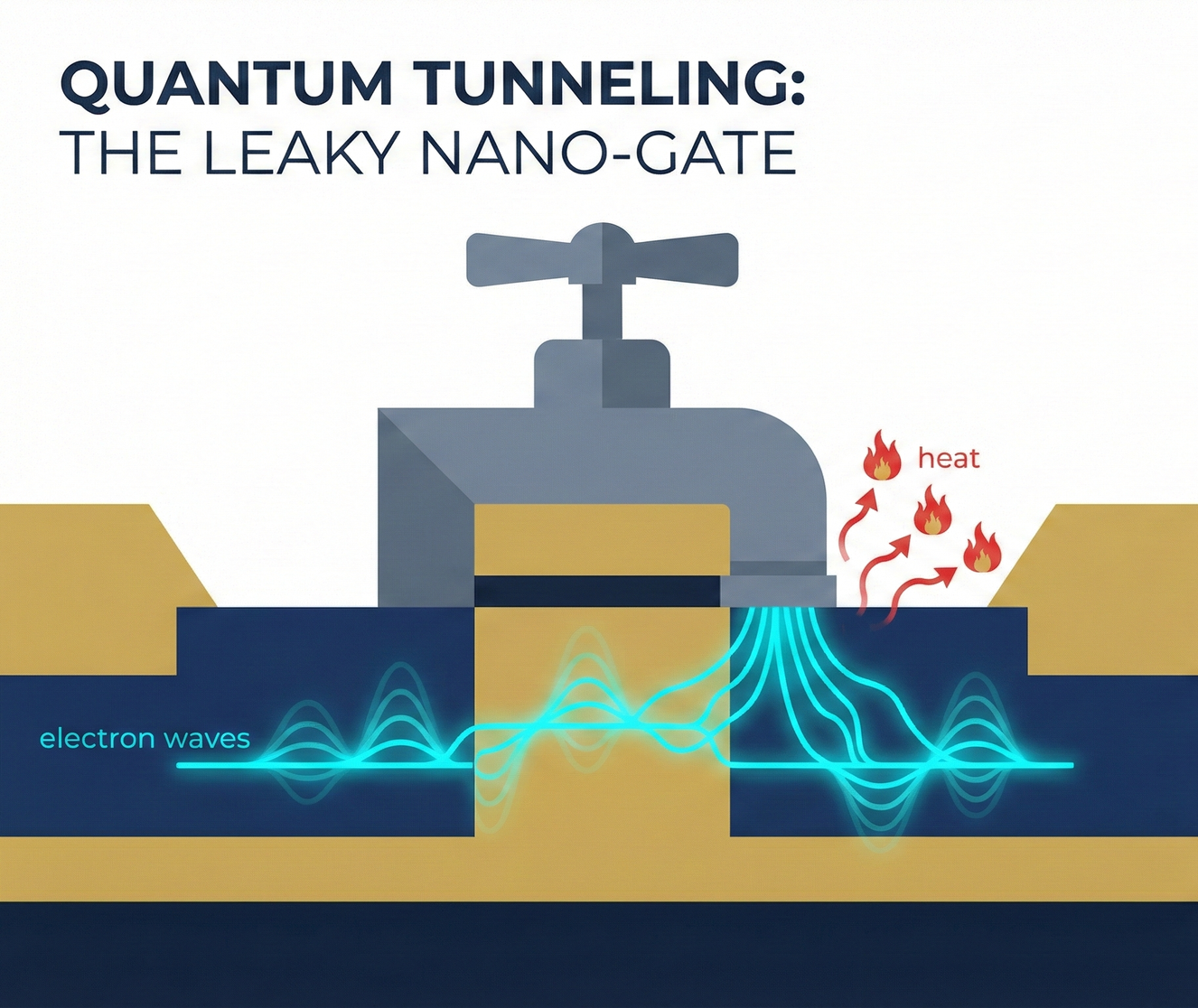
Semiconductors are able to perform computations because they contain tens of billions of "transistors." You can imagine a transistor as a floodgate (or a faucet). When the gate opens, current flows, representing "1"; when the gate closes, current stops, representing "0." Chips rely on the rapid switching of these tens of billions of 0s and 1s to play 4K videos, generate AI articles, or drive a Tesla.
For this system to function perfectly, there is one absolute prerequisite: when the gate is closed, the water (current) must be blocked "without a single drop leaking."
In the past, this wall blocking the water (the Gate Oxide) was very thick, making it easy to block electrons. But as processes advanced rapidly to 20 nanometers, and even 3 nanometers, this wall was stripped down to only a few atoms thick (approximately 1 to 2 nanometers).
At this point, something terrifying happened. At such thin scales, Newton's classical physics completely broke down, and Quantum Mechanics officially took over this world.
In the world of quantum mechanics, electrons are no longer just concrete "marbles"; they also possess wave-like properties. When the wall used to block electrons becomes extremely thin, the electron's wave function directly extends to the other side of the wall. The result is: electrons, like ghosts, disregard physical barriers and simply "tunnel through the wall."
This phenomenon is known in physics as Quantum Tunneling.
For semiconductor engineers, this isn't a cool sci-fi term; it's a disaster. It means: the faucet can't be shut tightly. Even when the system issues a "turn off (0)" command, and the gate is indeed closed, electrons mysteriously tunnel through the gate, continuing to flow. This unwanted current is what we call Leakage Current.
3. Dark Silicon Crisis: When a Skyscraper Becomes a High-Temperature Furnace
What are the consequences of leakage current? The answer is catastrophic waste heat.
Imagine your phone chip has 20 billion transistors. If every single transistor, when in the "off" state, is slightly leaking current, the sum of these 20 billion tiny leakages will generate an enormous amount of ineffective power consumption.
As soon as your phone turns on, even if it does nothing, the battery will drain rapidly, and the chip will become as hot as an iron. If the temperature gets too high, the chip will burn out. To solve this problem, mobile operating systems (like iOS or Android) are forced to activate "thermal throttling" protection mechanisms, forcibly reducing the chip's operating speed.
This leads to an utterly absurd phenomenon: the Dark Silicon effect. Foundries spend tens of billions of dollars to painstakingly pack tens of billions of super-powerful transistors onto a chip, but because of the risk of overheating and crashing, at any given moment, you can only activate 10% of these transistors to work, while the remaining 90% must be forced into "sleep mode." This is like building a 100-story, top-tier skyscraper, but due to the risk of electrical fires, only 10 floors can have their lights on simultaneously.
What kind of technological progress is this? This is the ultimate anxiety the entire tech industry faces when the blueprint reaches its limits.
4. Strategic Turning Point: Abandoning Patches for a Complete Architectural Revolution
At this juncture, decision-makers at TSMC and Intel understood a harsh truth: even if you drove ASML's engineers mad to create a lithography machine capable of etching 1-nanometer lines, you still wouldn't solve the leakage current problem. This is because it is a physical law of quantum mechanics, and humanity cannot overcome physical laws.
When the bricklayer's tools (equipment) have been pushed to their absolute limits, yet still cannot save a leaky building, there is only one solution: fire the bricklayers, bring in top structural architects, and completely dismantle and rebuild the entire building's steel framework.
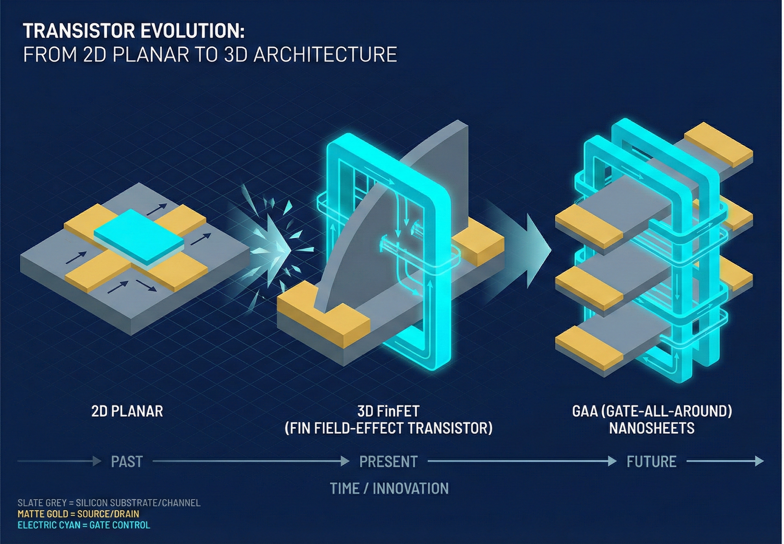
Since a 2D planar faucet will leak no matter how much it's pressed, we can no longer insist on "drawing planes smaller and smaller." We must switch our thinking to 3D spatial design. We must literally "pull" transistors, originally lying flat on the silicon wafer, to stand upright in mid-air; we even need to slice transistors into suspended nanometer-thin sheets, clamping them tightly from all directions to completely eliminate any possibility of electron escape.
This isn't sculpting; this is three-dimensional architectural engineering on a microscopic scale.
From Intel's first introduction of FinFET (Fin Field-Effect Transistor) in 2011, to Samsung and TSMC's full commitment to GAA (Gate-All-Around) in the 2-nanometer era by 2025, this is a magnificent history of "humanity's struggle against quantum leakage."
The cost of this architectural revolution is extremely high. Each transition in chip 3D structure means hundreds of billions of New Taiwan Dollars in R&D funding, hundreds of equipment replacements, and the deadly risk of yield collapse. Samsung once suffered a severe setback due to a rushed architectural transition, while TSMC, with a precise architectural gamble, has maintained its dominance for a decade.
Next, we will unveil this multi-hundred-billion-dollar architectural blueprint. We won't delve into obscure quantum mechanics formulas; we will use the simplest "faucet theory" to help you understand this century-defining transistor revolution from FinFET to GAA, and the life-and-death struggle for wafer foundry leadership hidden behind it.
In-depth Research · Quantitative Perspective
Want more quantitative research insights on semiconductors?
[Insight Subscription Plan] Say Goodbye to Retail Investor Thinking: Build Your Alpha Trading System with "Quantitative Chips" and "Consensus Data"EDGE Semiconductor Research
📍 Series Map — Navigate the Complete EDGE Semiconductor Research →


