We've finished looking at the top-grade asphalt (CCL copper clad laminate material) for paving signal highways. Now, let's turn our attention to the construction company responsible for building this overpass — PCB (Printed Circuit Board) manufacturers.
In the era of traditional PCs and servers over the past two to three decades, PCBs were always regarded by the capital markets as "traditional components" with low technological barriers, often even falling into price wars within the red supply chain. However, in the AI era, this green board is undergoing a violent "value re-rating."
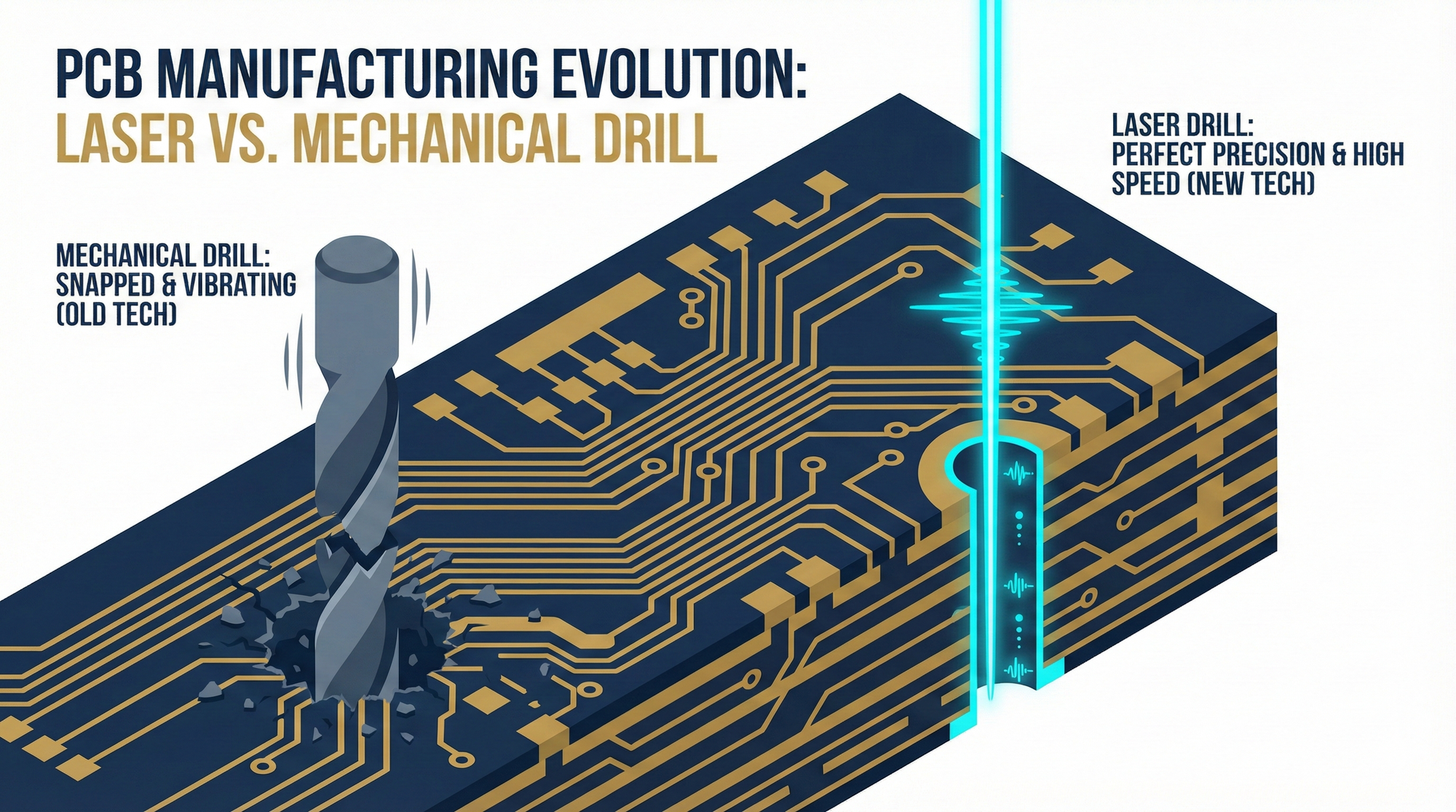
All these changes began with a broken drill bit.
🛑 Chapter One: The Physical Limits of Drill Bits
In traditional PCB manufacturing, the method for conducting electricity between different layers of circuitry was quite rudimentary: take an extremely fine mechanical drill bit and drill directly downwards from the surface of the board. However, in the world of AI servers, the data transfer volume between NVIDIA's GPUs and HBM (High Bandwidth Memory) is astronomical. To cope with this massive bandwidth, the pin density under the GPU has been pushed to the extreme, with distances between traces reduced to mere micrometers.
At this point, the physical limits emerged:
- The Destructive Nature of Vibration: If you use an extremely fine mechanical drill bit with a diameter of only 0.1 millimeters to drill holes at high speed, the drill bit will inevitably produce tiny physical vibrations (runout). In the past, no one cared about this minor vibration; but on AI substrates, this minute vibration can mercilessly sever the adjacent signal trace, which is finer than a human hair.
- The Verdict of Physical Limits: Mechanical drilling can no longer cope with the miniaturization speed of AI chips. PCB manufacturers were forced to abandon mechanical drill bits used for decades and switch to precision optical weapons — lasers.
This change officially declared that the manufacturing of server motherboards has entered an entirely new dimension.
⚡ Chapter Two: HDI (High Density Interconnect) — Cross-Industry Rescue by Mobile Phone Technology
The technology of using lasers for drilling is known in the industry as HDI (High Density Interconnect).
Interestingly, HDI was not invented for servers. It was previously an exclusive process for smartphones, especially Apple's iPhone. Due to the extremely limited internal space in mobile phones, thousands of tiny components had to be packed onto a board the size of a business card. Now, OAM (Compute Accelerator Modules) in AI servers, with their extremely high computational density and limited volume, are forced to "upgrade" to this incredibly expensive mobile phone manufacturing process.
So, what makes HDI so remarkable? It completely revolutionized the way "stairs" are built inside a PCB, an ultimate act of spatial magic:
1. Blind Via and Buried Via
- Traditional Through-Hole Boards: Previously, using mechanical drills meant drilling directly from the 1st layer all the way through to the 10th layer. This is like creating a "giant atrium" right in the middle of a 10-story building. This atrium occupies valuable floor space on every level, significantly reducing the area available for routing traces on each layer.
- HDI Laser Boards:
- Blind Via: Using a laser, a hole is precisely drilled from the surface (1st layer) and stops at the 2nd layer, leaving the space in layers 3 through 10 completely unaffected.
- Buried Via: Holes are drilled between internal layers, such as between the 3rd and 4th layers, connecting them without being visible from the exterior of the board.
- Space Optimization: This is akin to building "intricate hidden staircases" within a building. It significantly saves vertical space, allowing engineers to route tens of times more traces on the same board than before.
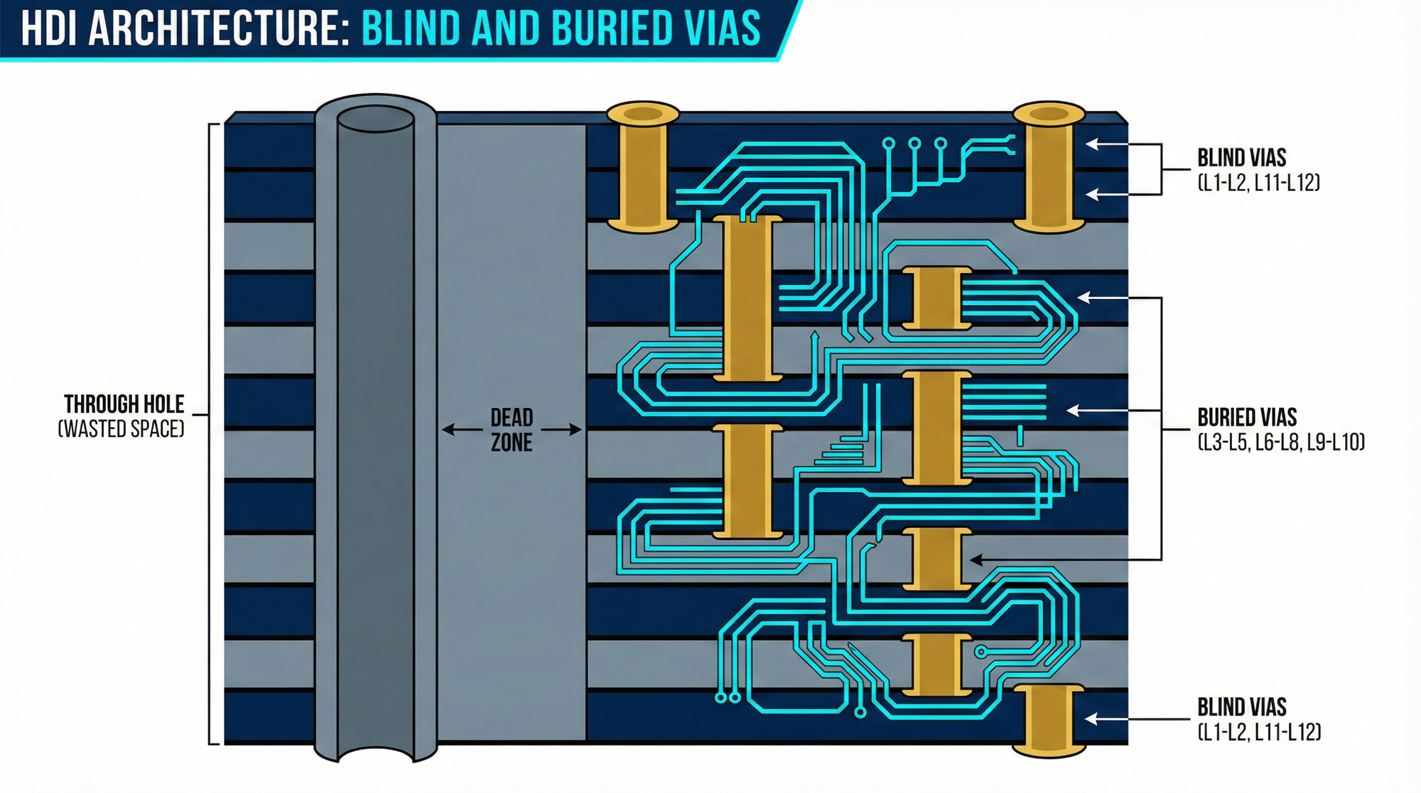
2. Any-layer HDI — The Pinnacle of Labyrinths
This is the jewel in the crown of HDI technology. In this type of board, holes can be freely drilled and connections made arbitrarily between any layers, creating circuitry that resembles a perfect 3D labyrinth.
- Manufacturing Hell: To create an Any-layer board, you cannot simply stack 10 layers and "press them flat all at once" as before. It must involve completing the first layer, laser drilling, electroplating with copper, then stacking the second layer, laser drilling again, electroplating again... undergoing an **endless cycle of N times of "lamination-laser drilling-electroplating."**
- Dimensionality Reduction Attack: The time required to manufacture one Any-layer HDI compute board is more than three times that of a traditional server board, and if any layer in the middle is misdrilled, the entire board is scrapped. This extreme technological barrier has made it exceedingly difficult for traditional server PCB manufacturers, who were only accustomed to making "large, thick boards." However, it has presented an excellent opportunity for manufacturers who previously specialized in high-end mobile phone boards (such as Compeq and Unimicron) to cross over, launch a "dimensionality reduction attack," and capture highly profitable AI orders.
🦕 Chapter Three: Dissecting the GB200 Behemoth — The Three Major Skeletons Valued at Three Million US Dollars
1. OAM (Compute Accelerator Module) — The Most Difficult Microscopic Labyrinth
- Its Location: This is the "small board" located directly beneath the GPU and HBM (High Bandwidth Memory).
- Specification Extremes: Despite its small size, it is the most circuit-dense and hottest area in the entire server. To accommodate the GPU's dense pins, OAM must use top-tier M8 materials and employ an extreme manufacturing process of 5-layer HDI or even Any-layer interconnect. The manufacturing difficulty of this board is comparable to high-end smartphone motherboards, which is why Compeq (2313), originally a mobile phone board manufacturer, was able to cross over and enter the AI battleground.
2. UBB (Universal Baseboard) — The Largest Aircraft Carrier by Area
- Its Location: This is a massive baseboard that hosts multiple GPUs (i.e., filled with OAM modules) and network chips.
- Specification Extremes: The challenge for UBB lies not in extremely fine laser holes, but in "perfect flatness across its thickness and area." This board is often 20 to 26 layers thick and extremely large. To bake 26 layers of different materials (including high-end non-adhesive PPO resin and smooth HVLP copper foil) in a high-temperature laminating press, and ensure "absolutely no warpage" after removal, severely tests a PCB manufacturer's experience with temperature control and pressure parameters.
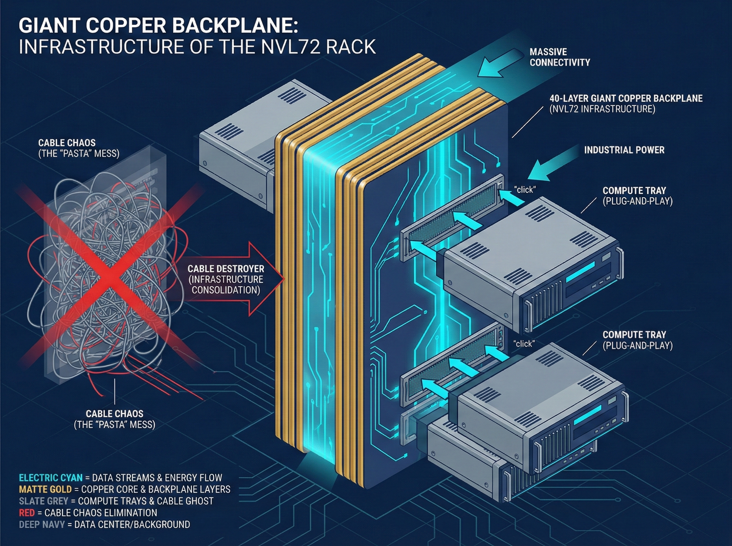
3. Backplane — The Counterattack of Copper and the Cable Terminator 🌟
This is a brand new, groundbreaking PCB making its debut in the GB200 NVL72 architecture, and it's the highest-priced single component in the entire rack.
- Its Ultimate Mission: Eliminate Spaghetti! In the previous generation H100 rack, data interconnection between GPUs required plugging in up to 5000 fiber optic or copper cables. The back of the entire rack was a tangled mess, resembling a huge pile of spaghetti, which not only made maintenance difficult but also severely impeded airflow for cooling.
- NVIDIA's Brutalist Aesthetics: This time, Jensen Huang decided to remove all cables and directly created an "enormously massive PCB copper backplane." All server compute trays slide in like drawers directly onto this giant backplane, achieving ultra-high-speed transmission of 1.8TB/s through the dense copper traces inside the backplane.
- Despair-Level Manufacturing Challenges:
- Thick as a Brick: This backplane has an astonishing 30 to over 40 layers.
- Registration Hell: Its size is immense, so much so that even standard PCB laminating presses cannot accommodate it. Even more daunting, when laminating this 30-layer behemoth, if a tiny drilled hole on the 1st layer is misaligned by just 0.1 millimeters (mm) relative to the 30th layer, the entire astonishingly expensive backplane is immediately deemed scrap.
🕳️ Chapter Four: The Invisible Killers — High Aspect Ratios and "Backdrill" Minimally Invasive Surgery
If you thought merely making boards thicker and drilling holes accurately was the end of it, you would underestimate the power of high-frequency physics. Thick boards (like UBBs and backplanes) face two manufacturing hurdles that make traditional PCB manufacturers shudder:
1. The Abyss of High Aspect Ratio
When a board is 30 layers thick (e.g., 4mm thick), but to save space, the hole diameter is only 0.2mm, it's like digging a "well 20 stories deep but only 1 meter in diameter" from the ground.
Not to mention the drill bit is extremely prone to breaking when digging (drilling), how do you then uniformly fill this abyss with "copper liquid (electroplating solution)" to the very bottom, allowing the hole wall to perfectly adhere to a layer of copper for electrical conduction? If even a tiny air bubble causes a break in the copper, the entire board becomes dysfunctional. This "deep hole electroplating" hurdle directly eliminated a large number of second-tier manufacturers.
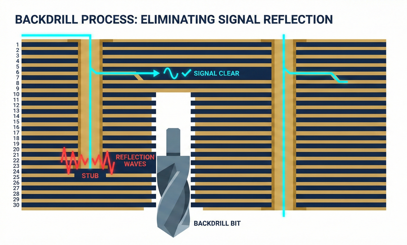
2. Backdrill — Precise Surgical Procedure
This is a classic challenge in high-frequency signal transmission. Suppose we have a conductive hole that penetrates a 30-layer board, but our high-frequency signal only needs to travel from the 1st layer to the 5th layer before turning off.
Then, the "superfluous copper tube" extending from the 5th layer down to the 30th layer is physically called a Stub.
- The Curse of the Appendix: Under ultra-high-frequency transmission, this extra copper tube acts like the "appendix" of the human body. When high-frequency signals rush into this appendix, they will hit the bottom and cause fatal "signal reflection," interfering with the normal signals being transmitted.
- The Limit of Minimally Invasive Surgery: To solve this problem, engineers must use a slightly larger drill bit from the back of the board (30th layer) to "precisely cut off" this redundant copper tube, and absolutely must not damage the useful traces on the 5th layer! This is like performing minimally invasive surgery blindfolded; if you drill a micro-millimeter too deep, the trace breaks, and this AI board, worth thousands of dollars, is immediately scrapped.
📊 4-2-5 Strategic Summary: Process Premium and Value Re-rating
Here's a summary for you. The PCB industry is undergoing an unprecedented "Value Re-rating."
Conclusion:
In the high-altitude operations of AI, PCBs are no longer just cheap plastic boards for routing traces, but high-tech works of art that combine precision optics (laser HDI), extreme chemistry (deep hole electroplating), and micrometer-level mechanical processing (backdrill). Whoever can stably control the yield rate of these 30-story boards will be able to command the most generous "process premium" from cloud giants.
In-depth Research · Quantitative Perspective
Want more semiconductor quantitative research insights?
【Insight Subscription Plan】Break Free from Retail Investor Mentality: Build Your Alpha Trading System with "Quantitative Chips" and "Consensus Data"EDGE Semiconductor Research
📍 Series Map — Navigate the Complete EDGE Semiconductor Research →


