Key Takeaway: 800V HVDC pushes silicon-based materials to their breakdown limits, thus SiC dominates the high-voltage backbone, and GaN occupies the high-frequency front end; however, SiC's physical Achilles' heel in mass production (micropipes) and its capital intensity have plunged the industry into a "war of attrition."
⚡ The Death Sentence for Silicon: Electrical Breakdown Under 800V High Voltage
In the previous article, we mentioned that engineers racked their brains to invent Super Junction technology, allowing silicon-based MOSFETs to barely hold the line below 48V.
However, recall NVIDIA's audacious directive aimed at completely eliminating heat loss from copper busbars within server racks: "Directly boost the voltage inside server racks to 800V high-voltage DC!"
When an extreme 800V high voltage relentlessly floods traditional silicon-based MOSFETs, the grim reaper of physics descends.
- Silicon material inherently has too narrow a "Bandgap"
- Under immense voltage pressure, electrons are forcibly stripped away
- Switches that should be insulated are instantaneously forced into conduction
In physics, this phenomenon is called: Dielectric Breakdown.
With a loud bang and a puff of white smoke, silicon-based MOSFETs are directly charred by the 800V high voltage.
In the ultimate high-voltage battleground of AI servers, silicon material has been sentenced to death.
To harness the furious energy of 800V, humanity must seek:
- Wider bandgaps
- Stronger bonds
- The ability to withstand extreme high voltages
These are the new elements. This is the destined stage for "Third-generation semiconductors (Wide Bandgap semiconductors)".
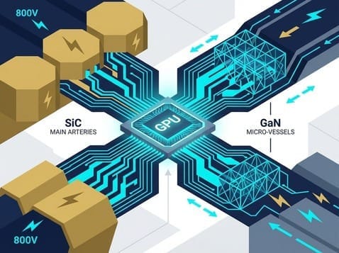
🗺️ Dividing the Domain: SiC and GaN Are Not Rivals, But Kings Ruling Their Own Territories
There is often a common misconception in the market that SiC (Silicon Carbide) and GaN (Gallium Nitride) are competing, and one will replace the other.
This is entirely a layman's misunderstanding.
In the power architecture of AI data centers, SiC and GaN have no intention of replacing each other. Instead, they perfectly "divide the domain" based on their respective extreme physical characteristics, each reigning supreme in different physical dimensions.
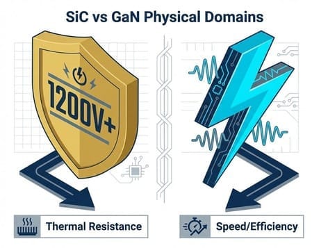
SiC (Silicon Carbide) = The Robust High-Voltage Artery
- Extremely "robust" physical properties
- Extremely strong atomic bonds
- Two major advantages:
- Ultra-high voltage resistance (easily exceeding 1200V, even 3300V and above)
- Extreme high-temperature resistance
Deployment Location: The most critical and highest voltage points in AI data centers.
From the giant HVDC (High Voltage Direct Current) rectifier cabinets outside the server room, all the way to the first high-voltage main valve within the rack for 800V → 48V conversion, SiC is an indispensable "efficiency heart."
Without it, 800V AI racks simply cannot operate.
GaN (Gallium Nitride) = The Agile High-Frequency Microcapillary
- Voltage resistance is inferior to SiC (typically below 650V)
- But possesses the highest electron mobility among all semiconductors
- Capable of switching at MHz-level high frequencies
- Generates almost no switching waste heat
Do you remember the "miniaturization magic" we discussed in the Lite-On Technology (6-1-3) article? GaN is the ultimate hero that enables transformers and inductors to drastically shrink in size.
Deployment Location: Within the rack for 48V → 12V, and even microscopic conversion to GPU chips.
GaN is the undisputed champion responsible for "slimming down" the server's internal components.
🌋 Micropipe Defects in the Crucible: SiC's Physical Achilles' Heel for Mass Production
To manufacture traditional silicon wafers, engineers simply melt silicon and, like pulling taffy, can easily draw out perfect 12-inch ingots.
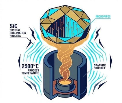
However, Silicon Carbide (SiC) is an extreme material, second only to diamond in hardness in nature; it simply "cannot be melted into a liquid"!
To grow an SiC ingot, high-purity carbon powder and silicon powder must be placed in an extremely hot graphite crucible exceeding 2500 degrees Celsius, allowing them to directly "sublimate" into gas, and then slowly crystallize by condensation at the top.
This process is called: Physical Vapor Transport (PVT).
Mass Production Challenges (Three Core Issues)
- Extremely slow crystal growth rate (only a few centimeters can be grown in several days)
- Extremely narrow process window (a temperature gradient difference of just a fraction of a degree can cause problems)
- Produces fatal defects: Micropipe Defects
These micropipes are like invisible hollow tunnels within the crystal ingot.
When this ingot is sliced into wafers and made into 800V high-voltage power components: if the component's circuit happens to lie over any micropipe, the component will instantly leak current, suffer dielectric breakdown, and be rendered scrap upon power-up.
This is why SiC yield rates have consistently been difficult to improve.
As the industry attempts to upgrade from 6-inch to 8-inch wafers to reduce costs, the edge stress and micropipe defects resulting from the increased area multiply exponentially, causing global major manufacturers to repeatedly delay their 8-inch mass production schedules.
🩸 The Fall of a Hegemon: Wolfspeed's Capital Scars and Chapter 11
When discussing SiC crystal growth, we must confront the former undisputed king of this track, the hegemon who controlled over 60% of the global SiC substrate lifeline—Wolfspeed.
In recent years, to widen its lead over competitors, Wolfspeed aggressively invested billions of dollars to build the world's largest 8-inch SiC plant in New York, USA.
They believed they could completely monopolize the EV and high-voltage power markets through the economies of scale from the 8-inch facility.
But capital markets are brutal, and the curse of physics is even more relentless.
Due to a disastrous failure in 8-inch facility yield rate ramp-up and utterly uncontrolled burn rate, coupled with unexpectedly sluggish demand in the global electric vehicle (EV) market, this erstwhile global hegemon was actually dragged down by heavy capital expenditures, forced into financial restructuring under Chapter 11 of the U.S. Bankruptcy Code.
This is an extremely shocking saga of industry struggles and hardship.
It announced to the world: SiC is a "death game that absolutely cannot be played without bottomless pockets."
🛟 AI Data Centers (AI DC): The Last Straw of Hope in Despair
However, even as Wolfspeed undergoes painful financial restructuring and the overall SiC environment is still rated as "Weak Environment" by foreign investors, a recent insight from Wall Street points to a glimmer of hope for the company's future:
"Although the overall environment is challenging, the immense business opportunities in AI data centers (AI DC) are strongly emerging (Opportunity Emerges)!"

Indeed, this refers to NVIDIA's ambitious 800V rack plan and the 380V HVDC high-voltage DC server rooms we discussed in 6-1-1.
When the electric vehicle market is no longer driving frantic procurement as it once did, AI computing infrastructure becomes the SiC industry's "sole and most certain" massive growth engine.
Wolfspeed's current strategy is to desperately cling to this lifeline of high-voltage AI server rooms, attempting to re-demonstrate the value of its crystal growth to the capital market with a new target model in the second half of 2026.
📉 Highpower (3707): The Reality of Persistent Losses and "Debunked" Narratives
If one were to look for a pure-play foundry in Taiwan with both SiC and GaN manufacturing capabilities, the first company everyone would think of is undoubtedly Highpower Optoelectronics (3707).
In the market's aspirational vision, Highpower, as one of the very few manufacturers in Taiwan capable of providing third-generation semiconductor foundry services, should ideally be swamped with orders amid the upgrade frenzy of AI server HVDC (High Voltage Direct Current) and 800V.
There was even a rumor circulating in the market that if Silicon Interposers in advanced packaging were to adopt SiC material in the future, Highpower would become the biggest winner.
However, the market promptly doused this dream with a bucket of ice water.
Highpower's current financial situation remains deeply mired in "persistent losses."
The foreign investment community was even more blunt in debunking market rumors: "The speculation about Silicon Interposers adopting SiC material is completely unrelated to Highpower's core business technology."
This reveals the most disheartening reality for SiC foundries in Taiwan: SiC is a game that places extreme emphasis on "economies of scale."
While major international players (such as Infineon, STMicroelectronics) are aggressively expanding their in-house 8-inch production capacity, foundries in Taiwan, if unable to achieve a decisive advantage in yield rates, will find it difficult to secure long-term orders from top-tier international manufacturers.
Although AI's HVDC indeed represents a massive potential contribution in the future, "potential" does not equate to "current reality."
With production utilization rates unable to be effectively filled and depreciation expenses being extremely heavy, Highpower is currently undergoing a painfully challenging period of capital consumption.
🚗 Actron (8255): A Difficult Transition from Automotive to Cloud
If Highpower represents the dilemma of wafer foundries, then Actron Technology (8255), a subsidiary of the Sino-American Silicon Products Group, represents the cruel pains of a "module manufacturer's transformation."
Actron was previously the dominant player in "automotive diodes" for traditional fuel-powered vehicles globally.
Facing the dual revolutions of electric vehicles and AI, Actron demonstrated great ambition, fully venturing into SiC high-efficiency rectifier modules and attempting to strongly integrate these high-voltage modules into the power supply chains of cloud servers.
The vision is grand, but reality is stark.
Actron's operations are encountering strong headwinds:
- Customer Procurement Slowdown and New Product Delays: Due to end-vehicle manufacturers becoming more conservative in their procurement, coupled with "delays" in the progress of new products (including high-end SiC modules) that were initially highly anticipated, its revenue momentum has stalled.
- Relentless Margin Squeeze: During the product transition period, Actron was hit by the dual impact of exchange rate fluctuations and rising raw material costs. Its quarterly gross margin was not only lower than the previous quarter but also "missed analyst expectations (GM miss)."
Actron is a good company, and its strategic direction (automotive electrification + AI server high-voltage power) is absolutely correct.
However, the leap from traditional silicon-based diodes to SiC power modules with extremely high barriers to entry means that the "learning curve" and "customer validation cycle" are much longer than the market imagined.
When the growth of old products stagnates, and high-margin new products are not yet ready to take over, this creates a "difficult transition" period that is agonizing for investors.
🗺️ Strategic Wrap-up: Who Can Survive This "War of Attrition"?
This is the true face of third-generation semiconductors.
When we look at NVIDIA's 800V vision, we know the ultimate outcome for SiC will be profoundly brilliant.
But before reaching that culmination, from Wolfspeed in the U.S. to Highpower and Actron in Taiwan, the entire SiC industry chain is enduring a "war of attrition" akin to purgatory.
This is a survival of the fittest, a competition to see:
- Whose cash flow is stronger
- Whose group support is more robust
- Who can endure until high-voltage orders for AI data centers truly achieve "explosive volume growth"
No one doubts the future of SiC, but the capital market only cares "now" if you can achieve viable yields and profitability.
🌪️ The Price of High Frequency: The Disaster of EMI (Electromagnetic Interference), an Invisible Killer
GaN (Gallium Nitride)'s physical gift lies in its extraordinarily high "electron mobility."
This enables it to switch at frequencies of millions of times per second (MHz).
The faster the switching speed, the smaller the transformers and inductors within the power module can be made. This is the ultimate secret behind how Lite-On Technology can help extract valuable space in AI server racks.
However, the laws of physics are always fair: "There's no such thing as a free lunch."
When GaN furiously switches tens of amperes of current on and off millions of times per second within a server chassis, it triggers a terrifying side effect that makes all hardware engineers cringe: severe EMI (Electromagnetic Interference) and high-frequency noise.
Imagine this: on a crowded AI server motherboard, right next to it are GPU signal lines performing extremely high-speed, low-latency transmission via PCIe Gen6 or even NVLink.
If the high-frequency electromagnetic noise generated by the GaN power module is not tightly contained, these noises will penetrate the GPU's neural network like invisible ghosts, instantly disrupting the originally precise "0s and 1s" digital signals.
Therefore, while GaN can miniaturize the core transformer, it severely tests power supply manufacturers (such as Delta Electronics, Lite-On Technology) on their:
- Anti-interference circuit design
- Mastery of tuning high-end filters
This is why, in the upcoming 6-2-4 battle, we must explore the "high-end MLCCs and common mode inductors" that act as breakwaters to absorb these fatal noises.
👑 The Invisible King: TSMC (2330) and the GaN-on-Si Foundry Hegemony
Having understood the high-frequency magic and cost of GaN, we must turn back to a fundamental business question: Who manufactures these powerful GaN chips?
If you examine the global market share of GaN power ICs, you will see the names of European and American IC design giants such as Navitas and EPC.
However, these giants are fabless; they do not build their own factories.
When you peel back these top-tier GaN chips to trace their original manufacturer, you will be astonished to discover: behind them stands the same unshakeable invisible hand—TSMC (2330).
Why TSMC? This involves an extreme process called GaN-on-Si (Gallium Nitride on Silicon).
SiC must be grown on expensive SiC substrates, which is why Wolfspeed went bankrupt.
But GaN is very clever; engineers discovered: a thin layer of GaN can be grown directly on inexpensive and high-capacity traditional silicon (Si) wafers.
This sounds perfect, but in practice, it's sheer hell.
Because GaN and silicon have entirely different "lattice constants" and "thermal expansion coefficients."
If you directly deposit GaN onto silicon, during the cooling process, the entire wafer will warp and crack (Wafer Bowing) due to severe thermal stress.
To solve this critical lattice mismatch, an extremely complex buffer layer must be laid between the two.
Conclusion: Globally, when it comes to perfecting GaN-on-Si epitaxy technology and achieving near-perfect yields in 6-inch or even 8-inch fabs, TSMC is second to none.
Analysts in the market focus daily on TSMC's 3nm, 2nm, and CoWoS capacities.
They almost entirely overlook the small fraction of revenue from "specialty processes" in TSMC's financial reports.
But it is this GaN foundry production line, overlooked by foreign investors, that quietly controls the throat of global high-frequency miniaturized power supplies.
Whether it's the high-efficiency power supplies in AI servers or the compact 100W GaN fast charger in your hand, what's pulsating inside is all TSMC's microscopic magic.
🗺️ Strategic Wrap-up: The Third-Generation Semiconductor Landscape Is Established, Prepare for the Direct Impact of di/dt!
With the revelation of TSMC's GaN hegemony, this extremely in-depth [6-2-2 800V's Core Driver: The Physical Battleground of Silicon Carbide (SiC) and Gallium Nitride (GaN)] finally concludes its grand strategic overview for you.
Let's once again survey this extreme physical map:
- SiC Camp: Bearing the extreme high voltages of 800V and 1200V, despite enduring the curse of low yields and the pains of capital intensity (Wolfspeed, Highpower, Actron), it is the absolutely indispensable heavy armor for high-voltage transformation in AI server rooms.
- GaN Camp: Under TSMC's yield rate protection, with its assassin-like agility for high-frequency miniaturization, it has completely liberated the precious space within server racks.
Now, we have the high-voltage SiC main arteries and the high-frequency GaN microcapillaries.
The current faucet is ready for you.
However, the real test begins the moment this massive and furious current truly rushes into the motherboard and directly charges towards the GPU chip.
We mentioned the terror of $di/dt$ (instantaneous current change rate) in 6-1-4.
When a Blackwell chip instantaneously draws 1000 amperes of current within a microsecond, relying solely on a faucet-like switch is absolutely insufficient. If power is supplied through only one channel, the voltage would instantly collapse and crash the system.
To salvage this 1000-ampere surge, the "Power Phases" on the motherboard have undergone an exponential explosion.
An ultimate inductor war, revolving around PMIC (Power Management ICs), TLVR (Trans-Inductor Voltage Regulators), and Vicor vertical power delivery, is brutally unfolding on the motherboard.
In-depth Research · Quantitative Perspective
Want more insights into semiconductor quantitative research?
【Insight Subscription Plan】Bid Farewell to Retail Investor Thinking: Build Your Alpha Trading System with "Quantitative Chips" and "Consensus Data"EDGE Semiconductor Research
📍 Series Map — Navigate the Complete EDGE Semiconductor Research →


